Paper I — Q2
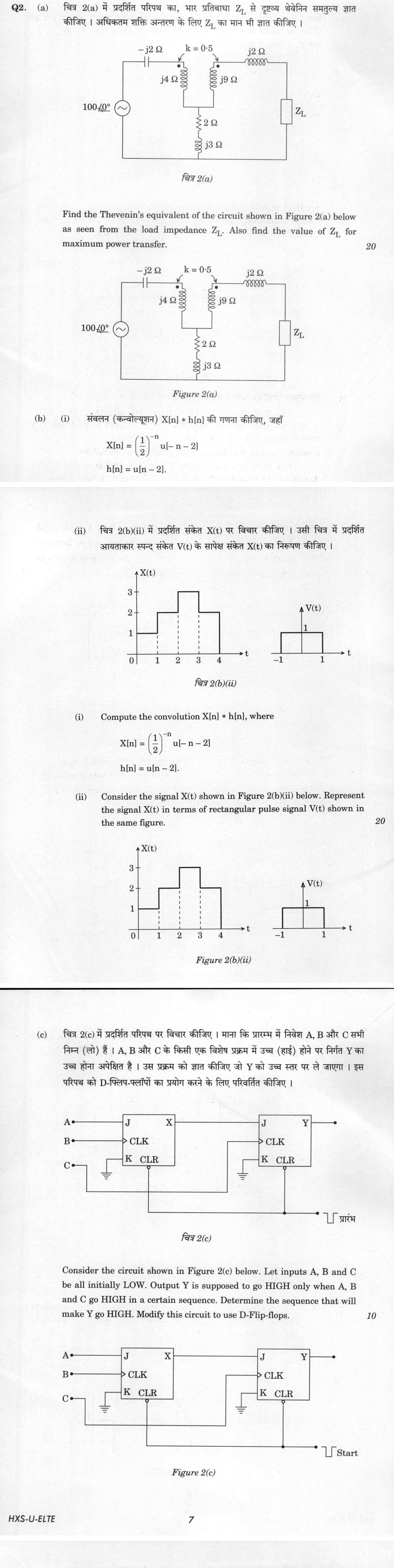
(a) Find the Thevenin's equivalent of the circuit shown in Figure 2(a) below as seen from the load impedance Z_L. Also find the…
Find the Thevenin's equivalent of the circuit shown in Figure 2(a) below as seen from the load impedance Z_L. Also find the value of Z_L for maximum power transfer. 20 marks
Compute the convolution X[n] * h[n], where X[n] = (1/2)^(-n) u[-n-2] h[n] = u[n-2].
Consider the signal X(t) shown in Figure 2(b)(ii) below. Represent the signal X(t) in terms of rectangular pulse signal V(t) shown in the same figure. 20 marks
Consider the circuit shown in Figure 2(c) below. Let inputs A, B and C be all initially LOW. Output Y is supposed to go HIGH only when A, B and C go HIGH in a certain sequence. Determine the sequence that will make Y go HIGH. Modify this circuit to use D-Flip-flops. 10 marks
हिंदी में प्रश्न पढ़ें
चित्र 2(a) में प्रदर्शित परिपथ का, भार प्रतिबाधा Z_L से दृश्य थेवेनिन समतुल्य ज्ञात कीजिए। अधिकतम शक्ति अंतरण के लिए Z_L का मान भी ज्ञात कीजिए। (20 अंक)
संवलन (कनवोल्यूशन) X[n] * h[n] की गणना कीजिए, जहाँ X[n] = (1/2)^(-n) u[-n - 2] h[n] = u[n - 2].
चित्र 2(b)(ii) में प्रदर्शित संकेत X(t) पर विचार कीजिए । उसी चित्र में प्रदर्शित आयताकार स्पंद संकेत V(t) के सापेक्ष संकेत X(t) का निरूपण कीजिए । (20 अंक)
चित्र 2(c) में प्रदर्शित परिपथ पर विचार कीजिए । माना कि प्रारंभ में निवेश A, B और C सभी निम्न (लो) हैं । A, B और C के किसी एक विशेष प्रक्रम में उच्च (हाई) होने पर निर्गत Y का उच्च होना अपेक्षित है । उस प्रक्रम को ज्ञात कीजिए जो Y को उच्च स्तर पर ले जाएगा । इस परिपथ को D-फ्लिप-फ्लॉपों का प्रयोग करने के लिए परिवर्तित कीजिए । (10 अंक)
The figure this question refers to, in words
The question paper is a scan and the diagram did not survive as text. This is the figure as read from the original page — every component, value and label — so the question can be worked from the text below.
(a) A circuit diagram showing a load impedance Z_L connected to a coupled-inductor network driven by an AC voltage source:
- Leftmost vertical branch contains an AC voltage source of 100/_0 degrees V.
- Top branch of the left loop contains a capacitor with impedance -j2 ohms connected in series between the positive/top terminal of the AC source and the top terminal of a coupled inductor.
- The left coupled inductor is vertical with impedance j4 ohms, having a dot at its top terminal.
- The right coupled inductor is vertical with impedance j9 ohms, having a dot at its top terminal.
- The two coupled inductors have a mutual coupling coefficient k = 0.5 indicated above them with a curved double-headed arrow.
- The bottom terminals of both coupled inductors (j4 ohms and j9 ohms) meet at a common junction node.
- From this common junction node, a vertical central branch goes down containing a series combination of a 2 ohm resistor and a j3 ohm inductor, connecting to the bottom reference rail.
- The bottom reference rail connects the negative/bottom terminal of the voltage source, the bottom of the 2 ohm + j3 ohm branch, and the bottom terminal of the load impedance Z_L.
- From the top terminal of the j9 ohm inductor, the top branch of the right loop continues horizontally through an inductor with impedance j2 ohms to the top terminal of the load impedance Z_L.
- The load impedance Z_L is connected vertically across the output terminals.
(b) Figure 2(b)(ii) consists of two waveforms plotted against time t:
- Signal X(t): Plot of X(t) versus t. The signal is piecewise constant and zero outside [0, 4]. For 0 <= t < 1, X(t) = 1; for 1 <= t < 2, X(t) = 2; for 2 <= t < 3, X(t) = 3; for 3 <= t < 4, X(t) = 2; and X(t) = 0 for t < 0 and t > 4. Dashed vertical grid lines extend down to the t-axis at t = 1, 2, and 3. The t-axis has labeled tick marks at 0, 1, 2, 3, 4, and the vertical axis has labeled tick marks at 1, 2, 3.
- Signal V(t): Plot of a rectangular pulse V(t) versus t. The pulse has an amplitude of 1 spanning from t = -1 to t = 1, and is 0 elsewhere. The horizontal axis is labeled at -1 and 1, and the vertical axis is labeled at 1.
(c) A digital circuit schematic titled 'Figure 2(c)' consisting of two JK flip-flops:
- First flip-flop (left):
- J input is connected to input terminal A.
- Clock (CLK) input is connected to input terminal B.
- K input is connected to ground.
- Active-low clear input (CLR with an inversion bubble) is connected to an active-low signal line labeled 'Start' (indicated with a negative pulse icon).
- Output Q is labeled X.
- Second flip-flop (right):
- J input is connected directly to the output X of the first flip-flop.
- Clock (CLK) input is connected to input terminal C.
- K input is connected to ground.
- Active-low clear input (CLR with an inversion bubble) is connected to the same 'Start' signal line as the first flip-flop.
- Output Q is labeled Y.
Model answer
Written by UPSC Answer Check against this question's marking rubric, to the expected length. UPSC does not publish answers for Mains — this is one way to score well, not an official key.
(a) Let the bottom rail be ground. Remove Z_L for open-circuit Thevenin voltage. Let i₁ and i₂ enter the dotted terminals of the j4 Ω and j9 Ω inductors. Mutual impedance: jωM = k√(ωL₁·ωL₂) = 0.5√(4×9) = j3 Ω.
Coupled-inductor equations: V₁ − Vₘ = j4i₁ + j3i₂ V₂ − Vₘ = j3i₁ + j9i₂
With Z_L open, i₂ = 0. The left branch gives: V₁ = 100 + j2i₁ Vₘ = (2 + j3)i₁
Thus: 100 + j2i₁ − (2 + j3)i₁ = j4i₁ 100 = (2 + j5)i₁ i₁ = 100/(2 + j5) A
The Thevenin voltage is V₂: Vth = Vₘ + j3i₁ = (2 + j6)i₁ Vth = 100(2 + j6)/(2 + j5) = (3400 + j200)/29 V
For Zth, kill the source and apply Vₜ at the load terminals. The j2 Ω branch gives i₂ = Iₜ and V₂ = Vₜ − j2Iₜ. The source side gives V₁ = j2i₁, and KCL at the common node gives Vₘ = (2 + j3)(i₁ + Iₜ). Using the coupled equations: i₁ = −Iₜ(2 + j6)/(2 + j5) Vₜ = Iₜ[(2 + j14) − (2 + j6)²/(2 + j5)] Therefore: Zth = (2 + j198)/29 Ω
For maximum power transfer, Z_L = Zth*: Zth = (2 + j198)/29 Ω, Vth = (3400 + j200)/29 V, Z_L = (2 − j198)/29 Ω.
(b)(i) Given: X[n] = (1/2)⁻ⁿu[−n−2] = 2ⁿu[−n−2], so X[n] = 2ⁿ for n ≤ −2, else 0. h[n] = u[n−2], so h[n] = 1 for n ≥ 2, else 0.
Convolution: Y[n] = Σₖ X[k]h[n−k] Nonzero when k ≤ −2 and n−k ≥ 2, i.e. k ≤ n−2. Hence: k ≤ min(−2, n−2)
So: Y[n] = sum from k = −∞ to min(−2, n−2) of 2ᵏ = 2^(min(−2, n−2)+1)
If n ≤ 0, min = n−2, so Y[n] = 2^(n−1). If n ≥ 1, min = −2, so Y[n] = 1/2.
Y[n] = 2^(n−1)u[−n] + (1/2)u[n−1].
(b)(ii) V(t) = 1 for −1 ≤ t ≤ 1, and 0 otherwise. The signal X(t) is: 1 on [0,1), 2 on [1,2), 3 on [2,3), 2 on [3,4), 0 elsewhere.
Using shifted V(t): X(t) = V(t−1) + V(t−2) + 2V(t−3)
Check:
- 0 ≤ t < 1: V(t−1)=1 ⇒ X=1
- 1 ≤ t < 2: V(t−1)+V(t−2)=2
- 2 ≤ t < 3: V(t−2)+2V(t−3)=1+2=3
- 3 ≤ t < 4: 2V(t−3)=2
X(t) = V(t−1) + V(t−2) + 2V(t−3). (Equality holds for all t except at the jumps t = 0,1,2,3,4, where endpoint values are immaterial.)
(c) Assume positive-edge-triggered flip-flops and Start normally HIGH; a LOW Start pulse clears both flip-flops.
First JK has J=A, K=0, clock=B. Its characteristic equation is: X⁺ = A + X
So X can become 1 only when B rises while A is already HIGH.
Second JK has J=X, K=0, clock=C: Y⁺ = X + Y
So Y can become 1 only when C rises while X is already HIGH. Since X is set by B after A, the required sequence is: A → B → C, i.e. A HIGH first, then B HIGH, then C HIGH.
D-flip-flop modification:
- Replace first JK by D flip-flop with D₁ = A + X, clock B, clear Start, output X.
- Replace second JK by D flip-flop with D₂ = X + Y, clock C, clear Start, output Y.
- Use OR gates to form D₁ and D₂.
This gives Q⁺ = D = J + Q, exactly matching the original JK operation with K=0.
What "Solve" is asking you to do
Choose the method, then carry it through to a final answer. Identifying what kind of problem this is and why that method applies is the first thing marked; a correct figure arrived at invisibly earns almost nothing.
Structure that answers it
Given data and what is required → method chosen, with the reason it applies → set-up (equation, circuit, free body, trial balance) → working, step by step → answer with units and any condition of validity
Where marks are lost
Doing the middle steps mentally and writing only the result. In mathematics papers, a further loss comes from giving a decimal where the exact value in surds or fractions was wanted, or from skipping the justification a part explicitly asks for.
How this answer will be evaluated
Approach
(a) calculate: given > formula > substitution > result with units > interpretation | (b(i)) calculate: given > formula > substitution > result with units > interpretation | (b(ii)) describe: define > structure or process in order > labelled diagram > significance | (c) trace: start point > the stages in sequence > end point > what changed Full marks: Complete working with correct equivalent circuits, all steps shown, final answers with units, and clear diagrams.
Key points expected
- Redraw circuit with mutual inductance (k=0.5) marked
- Calculate Thevenin voltage V_th across Z_L terminals
- Calculate Thevenin impedance Z_th looking into terminals
- State Z_L = Z_th* for maximum power transfer
- Identify support ranges of X[n] and h[n]
- Set up convolution sum with correct limits
- Evaluate sum for all relevant n values
- Present result as piecewise or closed-form expression
Evaluation rubric
Each sub-part is marked on its own, against the marks and word limit printed on the paper.
- (a) Thevenin equivalent circuit and Z_L for maximum power transfer. 20 marks
calculate— given → formula → substitution → result with units → interpretation
Must cover
- Redraw circuit with mutual inductance (k=0.5) marked
- Calculate Thevenin voltage V_th across Z_L terminals
- Calculate Thevenin impedance Z_th looking into terminals
- State Z_L = Z_th* for maximum power transfer
Loses marks
- Sign errors in mutual inductance terms
- Missing equivalent circuit diagram
- Formula application without circuit analysis
Earns more
- Correct handling of coupled inductor dot convention
- Phasor diagram for voltage/current relationships
- Step-by-step mesh or nodal analysis shown
- Final values with correct units (Ω, V)
Extra mark
- Verification using alternative method (e.g., open-circuit/short-circuit)
- Comment on power factor or reactive power
- (b(i)) Convolution X[n] * h[n] for given discrete signals.
calculate— given → formula → substitution → result with units → interpretation
Must cover
- Identify support ranges of X[n] and h[n]
- Set up convolution sum with correct limits
- Evaluate sum for all relevant n values
- Present result as piecewise or closed-form expression
Loses marks
- Incorrect limits in convolution sum
- Sign errors in (1/2)^(-n) term
- Missing intermediate summation steps
Earns more
- Correct handling of unit step functions u[-n-2] and u[n-2]
- Geometric series summation shown explicitly
- Result plotted or tabulated for clarity
- Verification at boundary points
Extra mark
- Z-transform method as cross-check
- Comment on causality or stability of result
- (b(ii)) Representation of X(t) using rectangular pulse V(t).
describe— define → structure or process in order → labelled diagram → significance
Must cover
- Identify V(t) as unit rectangular pulse from -1 to 1
- Express X(t) as sum of scaled and shifted V(t)
- Determine correct amplitudes and time shifts
- Write final expression X(t) = Σ a_k V(t - t_k)
Loses marks
- Incorrect pulse width or shift values
- Missing scaling factors
- No final closed-form expression
Earns more
- Correct identification of pulse widths and positions
- Clear labeling of each component pulse
- Verification by sketching the sum
- Use of standard notation for shifted pulses
Extra mark
- Alternative representation using derivative or integral
- Comment on energy or power of the signal
- (c) Sequence for Y HIGH and D-Flip-flop circuit modification. 10 marks
trace— start point → the stages in sequence → end point → what changed
Must cover
- Trace state transitions through J-K flip-flops
- Determine exact sequence of A, B, C going HIGH
- Show state table or timing diagram
- Redraw circuit using D-Flip-flops with correct logic
Loses marks
- Incorrect state transition sequence
- Missing D-Flip-flop conversion logic
- No clear final circuit diagram
Earns more
- Clear state transition diagram
- Correct conversion from J-K to D flip-flop equations
- Labeled inputs and outputs in modified circuit
- Verification of sequence with timing diagram
Extra mark
- Comment on circuit complexity or gate count
- Simplification of logic using K-map or Boolean algebra
Practice this exact question
Write your answer and it is marked point by point against the model answer above — what you covered, what you missed, what you got wrong.
Evaluate my answer →More from Electrical Engineering 2021 Paper I
- Q1 (a) In Figure 1(a) shown below, the two-port network is characterized in terms of y-param…
- Q2 (a) Find the Thevenin's equivalent of the circuit shown in Figure 2(a) below as seen from…
- Q3 (a) (i) Explain what happens when a circuit shown in Figure 3(a)(i) below is constructed…
- Q4 (a) Consider a discrete time system with transfer function given by H(z) = Y(z)/R(z) = (z…
- Q5 (a) A step down dc chopper is feeding a load of R = 10 Ω and L = 20 mH. The dc supply vol…