Paper I — Q4
(a) Consider a discrete time system with transfer function given by H(z) = Y(z)/R(z) = (z⁻¹ - ½z⁻²)/(1 - z⁻¹ + 2/9…
Consider a discrete time system with transfer function given by
H(z) = Y(z)/R(z) = (z⁻¹ - ½z⁻²)/(1 - z⁻¹ + 2/9 z⁻²).
Calculate the following :
The impulse response of the system
The step response of the system with zero initial conditions
The step response of the system with initial conditions y[-1] = 1 and y[-2] = 2 20
Verify by determining the logic equation for the output and by constructing the truth table for the logic circuit shown in Figure 4(b).
Use an 8 to 1 multiplexer and logic gates to implement the following function :
F(A, B, C, D, E) = Σ m (0, 1, 2, 4, 5, 6, 7, 13, 14, 20, 21, ..., 28, 29, 30, 31)
20
Figure 4(b)
Determine the closed loop gain of the inverting amplifier shown in Figure 4(c) below. Explain the result if R₁ → 0 or R₃ → 0.
10
हिंदी में प्रश्न पढ़ें
H(z) = Y(z)/R(z) = (z⁻¹ - ½z⁻²)/(1 - z⁻¹ + 2/9 z⁻²) द्वारा प्रदर्शित अंतरण फलन वाले एक असतत समय तंत्र पर विचार कीजिए तथा निम्नलिखित की गणना कीजिए :
तंत्र की आवेग अनुक्रिया
शून्य प्रारंभिक स्थिति के लिए तंत्र की पद अनुक्रिया
प्रारंभिक स्थिति y[-1] = 1 तथा y[-2] = 2 के लिए तंत्र की पद अनुक्रिया
चित्र 4(b) में प्रदर्शित तार्किक परिपथ का सत्यापन, तार्किक समीकरण ज्ञात करके तथा सत्यता तालिका निर्माण करके कीजिए।
एक 8 से 1 बहुलक (मल्टीप्लेक्सर) तथा तार्किक द्वारों का प्रयोग निम्नलिखित फलन का कार्यान्वयन करने के लिए कीजिए :
F(A, B, C, D, E) = Σ m (0, 1, 2, 4, 5, 6, 7, 13, 14, 20, 21, ..., 28, 29, 30, 31)
चित्र 4(c) में प्रदर्शित प्रतिप प्रवर्धक (इनवर्टिंग एम्पलीफायर) की बंद पाश लब्धि का मान ज्ञात कीजिए । R₁ → 0 या R₃ → 0 की स्थिति में परिणाम की व्याख्या कीजिए ।
चित्र 4(c)
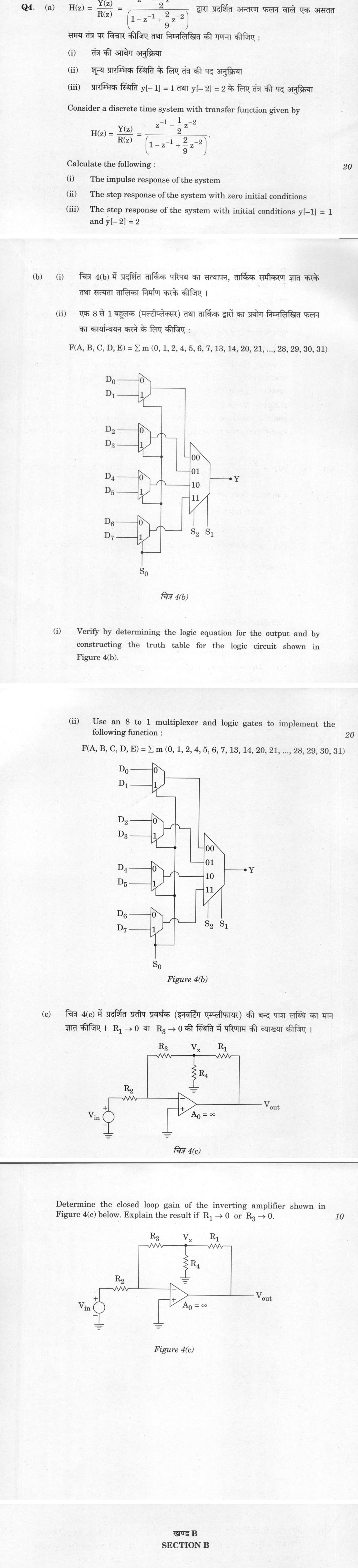
The figure this question refers to, in words
The question paper is a scan and the diagram did not survive as text. This is the figure as read from the original page — every component, value and label — so the question can be worked from the text below.
(b) A logic circuit diagram labeled Figure 4(b). The circuit consists of four 2-to-1 multiplexers on the left feeding into a single 4-to-1 multiplexer on the right. The 4-to-1 multiplexer has select inputs labeled S2 and S1, and an output labeled Y. The select inputs S2 and S1 are connected to the outputs of the first and third 2-to-1 multiplexers, respectively. The first 2-to-1 multiplexer has data inputs D0 and D1, and its select input is connected to S0. The second 2-to-1 multiplexer has data inputs D2 and D3, and its select input is connected to S0. The third 2-to-1 multiplexer has data inputs D4 and D5, and its select input is connected to S0. The fourth 2-to-1 multiplexer has data inputs D6 and D7, and its select input is connected to S0. The output of the first 2-to-1 multiplexer is connected to the 00 input of the 4-to-1 multiplexer. The output of the second 2-to-1 multiplexer is connected to the 01 input of the 4-to-1 multiplexer. The output of the third 2-to-1 multiplexer is connected to the 10 input of the 4-to-1 multiplexer. The output of the fourth 2-to-1 multiplexer is connected to the 11 input of the 4-to-1 multiplexer. There is a common input line labeled S0 connected to the select inputs of all four 2-to-1 multiplexers.
(c) An inverting operational amplifier circuit. The op-amp has infinite open-loop gain (A0 = infinity). The non-inverting input terminal is connected to ground. The inverting input terminal is connected to a node where three branches meet: 1) An input branch from a voltage source Vin through a resistor R2. 2) A feedback branch from the output node Vout through a resistor R1. 3) A branch through a resistor R3 to a node labeled Vx. The node Vx is connected to ground through a resistor R4. The output of the op-amp is labeled Vout.
What "Calculate" is asking you to do
Apply the standard formula or schedule to data the question has already supplied — a table of readings, cost records, a balance sheet — and produce the number. The method is rarely in doubt; the marks sit in the named intermediate quantities, each of which has to appear as a labelled line.
Structure that answers it
Data as given → formula or standard treatment, named → substitution → each intermediate, labelled → result with units
Where marks are lost
Omitting an intermediate the marking scheme pays for separately, or rounding at an intermediate line so the final figure drifts. In commerce and accountancy, any figure in a statement that no numbered working note supports is treated as unearned.
How this answer will be evaluated
Approach
(a) calculate: given > formula > substitution > result with units > interpretation | (b) describe: define > structure or process in order > labelled diagram > significance | (c) calculate: given > formula > substitution > result with units > interpretation Full marks: Complete derivations with correct logic and clear explanations of all limiting cases.
Key points expected
- Factorize denominator to find system poles
- Perform partial fraction expansion of H(z)
- Apply inverse Z-transform for impulse response
- Account for initial conditions y[-1] and y[-2]
- Derive the logic equation for the output Y
- Construct the complete truth table for the circuit
- Map the 5-variable function to the 8-to-1 MUX inputs
- Identify the correct select lines and data inputs
Evaluation rubric
Each sub-part is marked on its own, against the marks and word limit printed on the paper.
- (a) Impulse and step responses of the discrete system for zero and non-zero initial conditions. 20 marks
calculate— given → formula → substitution → result with units → interpretation
Must cover
- Factorize denominator to find system poles
- Perform partial fraction expansion of H(z)
- Apply inverse Z-transform for impulse response
- Account for initial conditions y[-1] and y[-2]
Loses marks
- Incorrect partial fraction expansion
- Ignoring the initial conditions in part (iii)
- Sign errors in the difference equation
Earns more
- Correct identification of pole locations
- Explicit calculation of partial fraction coefficients
- Clear distinction between zero-state and zero-input response
Extra mark
- Verification of stability based on pole locations
- (b) Verification of the logic circuit and implementation of a 5-variable function using an 8-to-1 MUX. 20 marks
describe— define → structure or process in order → labelled diagram → significance
Must cover
- Derive the logic equation for the output Y
- Construct the complete truth table for the circuit
- Map the 5-variable function to the 8-to-1 MUX inputs
- Identify the correct select lines and data inputs
Loses marks
- Incorrect truth table entries
- Wrong assignment of select lines for the MUX
- Failure to account for all minterms in the function
Earns more
- Correct simplification of the logic equation
- Accurate mapping of minterms to MUX data inputs
- Clear labeling of the multiplexer diagram
Extra mark
- Use of K-map to simplify the function before implementation
- (c) Closed-loop gain of the inverting amplifier and analysis of limiting cases R1→0 and R3→0. 10 marks
calculate— given → formula → substitution → result with units → interpretation
Must cover
- Apply KCL at the inverting node (virtual ground)
- Derive the expression for Vout/Vin
- Analyze the circuit behavior when R1 approaches 0
- Analyze the circuit behavior when R3 approaches 0
Loses marks
- Incorrect application of KCL at the inverting node
- Failure to explain the physical significance of the limiting cases
- Sign errors in the gain expression
Earns more
- Correct application of the virtual ground concept
- Clear explanation of the physical meaning of the limiting cases
- Proper handling of the feedback network
Extra mark
- Discussion of the effect of R4 on the circuit
Model answer coming soon
Every evaluation on this site is marked against a verified model answer. This question's answer is still being written; evaluation opens the moment it lands.
More from Electrical Engineering 2021 Paper I
- Q1 (a) In Figure 1(a) shown below, the two-port network is characterized in terms of y-param…
- Q2 (a) Find the Thevenin's equivalent of the circuit shown in Figure 2(a) below as seen from…
- Q3 (a) (i) Explain what happens when a circuit shown in Figure 3(a)(i) below is constructed…
- Q4 (a) Consider a discrete time system with transfer function given by H(z) = Y(z)/R(z) = (z…
- Q5 (a) A step down dc chopper is feeding a load of R = 10 Ω and L = 20 mH. The dc supply vol…
- Q6 (a) The magnetic field intensity of a linearly polarized uniform plane wave propagating i…
- Q7 The following test data are obtained for a three-phase, 195 MVA, 15 kV, 50 Hz star connec…