Paper I — Q4
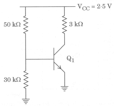
(a) For the circuit shown below, early voltage V_A = ∞ and β = 100. Find the reverse saturation current if: (i) the collector…
For the circuit shown below, early voltage V_A = ∞ and β = 100. Find the reverse saturation current if:
the collector current of Q₁ = 0·5 mA.
Q₁ is biased at the edge of saturation. 20 marks
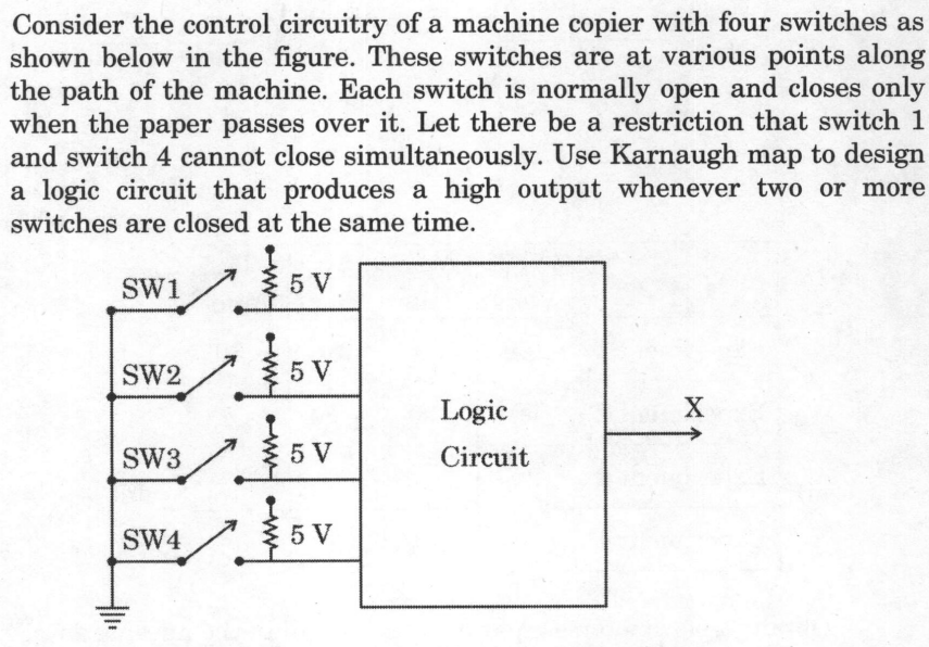
Consider the control circuitry of a machine copier with four switches as shown below in the figure. These switches are at various points along the path of the machine. Each switch is normally open and closes only when the paper passes over it. Let there be a restriction that switch 1 and switch 4 cannot close simultaneously. Use Karnaugh map to design a logic circuit that produces a high output whenever two or more switches are closed at the same time.
(SW1, SW2, SW3, SW4 : Switch 1, Switch 2, Switch 3, Switch 4) 20 marks
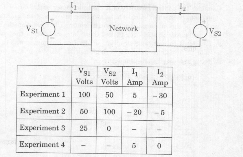
The experimental data for the two-port network shown in the figure is given in the table.
| V_S1 Volts | V_S2 Volts | I_1 Amp | I_2 Amp | |
|---|---|---|---|---|
| Experiment 1 | 100 | 50 | 5 | -30 |
| Experiment 2 | 50 | 100 | -20 | -5 |
| Experiment 3 | 25 | 0 | — | — |
| Experiment 4 | — | — | 5 | 0 |
Obtain Z-parameters, Y-parameters and fill in the missing data. 10 marks
हिंदी में प्रश्न पढ़ें
नीचे प्रदर्शित किए गए परिपथ के लिए, अर्ली बोल्टता V_A = ∞ तथा β = 100 है । व्युत्क्रम संतृप्ति धारा ज्ञात कीजिए यदि :
Q₁ की संग्राहक धारा 0·5 mA है ।
Q₁ संतृप्तता के छोर पर बायस्ड है । 20 marks
नीचे चित्र में दी गई चार सिवचों के साथ प्रतिलिपिक यंत्र की नियंत्रक परिपथिकी पर विचार कीजिए । ये सिवच यंत्र के मार्ग में विभिन्न बिन्दुओं पर स्थित हैं । प्रत्येक सिवच सामान्यतः खुला रहता है और केवल तब बंद होता है, जब उसके ऊपर से कागज़ गुज़रता है । सिवच 1 तथा सिवच 4 का एक साथ बंद होना प्रतिबंधित है । कारना मानचित्र का उपयोग करते हुए एक तर्क परिपथ अभिकल्पित कीजिए जो दो अथवा दो से अधिक सिवचों के एक साथ बंद होने की दशा में उच्च निगत उत्पन्न करे ।
(SW1, SW2, SW3, SW4 : सिवच 1, सिवच 2, सिवच 3, सिवच 4) 20 marks
चित्र में प्रदर्शित द्वि-प्रदार तंत्र के लिए प्रयोगात्मक आँकड़े तालिका में दिए गए हैं।
Z-प्राचल, Y-प्राचल ज्ञात कीजिए तथा तालिका में अनुपलब्ध आँकड़े भरिए।
| V_S1 Volts | V_S2 Volts | I_1 Amp | I_2 Amp | ||
|---|---|---|---|---|---|
| प्रयोग 1 | 100 | 50 | 5 | -30 | |
| प्रयोग 2 | 50 | 100 | -20 | -5 | |
| प्रयोग 3 | 25 | 0 | — | — | |
| प्रयोग 4 | — | — | 5 | 0 | (10 marks) |
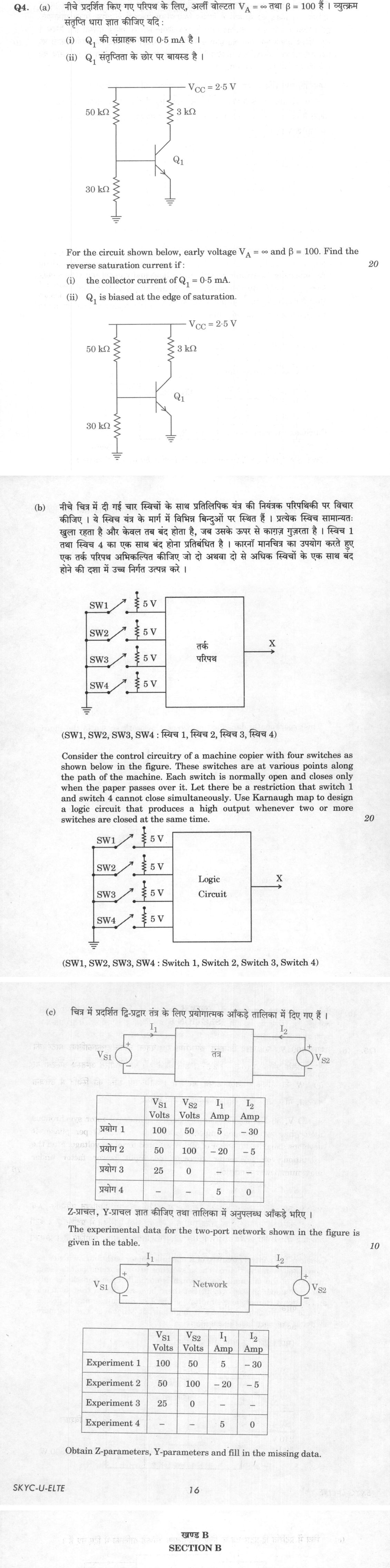
The figures printed on the question paper
Cut from the original 2023 Electrical Engineering paper, exactly as the candidates in the hall saw them.
The figure this question refers to, in words
The question paper is a scan and the diagram did not survive as text. This is the figure as read from the original page — every component, value and label — so the question can be worked from the text below.
(a) A DC circuit schematic with an NPN transistor Q1. A power supply rail at the top is labelled V_CC = 2.5 V. Connected to this rail are two parallel branches: The left branch consists of a 50 kOmega resistor in series with a 30 kOmega resistor connected to ground, forming a voltage divider. The base of transistor Q1 is connected to the junction between the 50 kOmega and 30 kOmega resistors. The right branch consists of a 3 kOmega resistor connected between the V_CC rail and the collector of Q1. The emitter of Q1 is connected directly to ground.
(b) A rectangular block representing an absorber material is placed vertically in free space. The left vertical surface of the absorber material is exposed to free space, where a horizontal arrow pointing to the right is labeled 'Incident wave' indicating a wave normally incident on the absorber. Directly attached to the right vertical surface of the absorber material is a shaded vertical strip labeled 'Conducting sheet'. A double-ended horizontal arrow spanning the thickness of the absorber material is labeled 'Absorber material'.
(c) The figure consists of two parts for a sequential digital circuit:
- Truth Table: A table with headers under two main categories:
- Inputs: 'CK', 'CLR_bar', 'Load'
- Next State: 'Q3', 'Q2', 'Q1', 'Q0' Rows:
- Row 1: CK = X, CLR_bar = 0, Load = X, Next State entries (Q3, Q2, Q1, Q0) are blank.
- Row 2: CK shows a rising-edge symbol, CLR_bar = 1, Load = 0, Next State entries are blank.
- Row 3: CK shows a rising-edge symbol, CLR_bar = 1, Load = 1, Next State entries are blank.
- Timing Diagram: A timing diagram showing 11 clock cycles with vertical dashed grid lines aligned to each of the 11 rising edges of CK (labeled 1 through 11):
- CK: Periodic square wave with 11 clock pulses.
- CLR_bar: Starts at logic HIGH, remains HIGH across rising edges 1 through 10, then transitions to logic LOW between rising edges 10 and 11, remaining LOW through rising edge 11.
- Load: Starts LOW, transitions to HIGH before rising edge 1, stays HIGH through rising edge 1, and drops to LOW before rising edge 2, remaining LOW for the remainder of the diagram.
- X_L: Starts LOW, remains LOW through rising edges 1 to 6; goes HIGH between edges 6 and 7, stays HIGH through edges 7 and 8, and transitions back to LOW between edges 8 and 9, remaining LOW thereafter.
- Q0, Q1, Q2, Q3: Four horizontal blank guide lines labeled Q0, Q1, Q2, Q3 provided to draw the output state waveforms.
Model answer
Written by UPSC Answer Check against this question's marking rubric, to the expected length. UPSC does not publish answers for Mains — this is one way to score well, not an official key.
(a)(i) Thevenin equivalent of the base divider: V_BB = 2.5 × 30/(50+30) = 15/16 V = 0.9375 V. R_BB = 50 kΩ || 30 kΩ = 18.75 kΩ.
Given I_C = 0.5 mA and β = 100: I_B = I_C/β = 0.5 mA/100 = 5 μA.
Base loop: V_BE = V_BB − I_B R_BB = 0.9375 − (5×10⁻⁶)(18.75×10³) = 0.84375 V.
For a BJT, I_C = I_S exp(V_BE/V_T). Taking V_T = 26 mV = 0.026 V: I_S = I_C exp(−V_BE/V_T) = (0.5×10⁻³) exp(−0.84375/0.026) = (0.5×10⁻³) exp(−32.4519) ≈ 4.03×10⁻¹⁸ A.
Final: I_S ≈ 4.0×10⁻¹⁸ A.
(a)(ii) At the edge of saturation, V_CB = 0, so V_C = V_B = V_BE. Collector current: I_C = (V_CC − V_BE)/R_C = (2.5 − V_BE)/3 kΩ. Base current: I_B = I_C/β = (2.5 − V_BE)/300 kΩ. Also, I_B = (V_BB − V_BE)/R_BB = (0.9375 − V_BE)/18.75 kΩ.
Equating: (0.9375 − V_BE)/18.75 = (2.5 − V_BE)/300. Solving gives V_BE = 5/6 V = 0.8333 V.
Then: I_C = (2.5 − 5/6)/3 mA = (10/6)/3 mA = 5/9 mA ≈ 0.5556 mA.
I_S = I_C exp(−V_BE/V_T) = (5/9×10⁻³) exp(−(5/6)/0.026) ≈ (5.5556×10⁻⁴) exp(−32.0513) ≈ 6.68×10⁻¹⁸ A.
Final: I_S ≈ 6.68×10⁻¹⁸ A.
(b) Let A = SW1, B = SW2, C = SW3, D = SW4. Output F = 1 whenever two or more switches are closed. The restriction A D = 1 is invalid, so minterms 9, 11, 13, 15 are don't-cares. Valid minterms for F = 1 are 3, 5, 6, 7, 10, 12, 14.
K-map groupings:
- m3, m7, m11, m15 → C D
- m5, m7, m13, m15 → B D
- m6, m7, m14, m15 → B C
- m10, m11, m14, m15 → A C
- m12, m13, m14, m15 → A B
Therefore: F = A B + A C + B C + B D + C D.
Final: F = SW1·SW2 + SW1·SW3 + SW2·SW3 + SW2·SW4 + SW3·SW4. Implement using five 2-input AND gates feeding a 5-input OR gate. The invalid state SW1 = SW4 = 1 is treated as don't-care.
(c) Using the standard two-port convention: V₁ = Z₁₁ I₁ + Z₁₂ I₂, V₂ = Z₂₁ I₁ + Z₂₂ I₂.
From experiments 1 and 2: 100 = 5 Z₁₁ − 30 Z₁₂, 50 = −20 Z₁₁ − 5 Z₁₂. Solving gives Z₁₁ = −8/5 Ω, Z₁₂ = −18/5 Ω.
50 = 5 Z₂₁ − 30 Z₂₂, 100 = −20 Z₂₁ − 5 Z₂₂. Solving gives Z₂₁ = −22/5 Ω, Z₂₂ = −12/5 Ω.
So: Z = [[−8/5, −18/5], [−22/5, −12/5]] Ω.
Determinant: ΔZ = (−8/5)(−12/5) − (−18/5)(−22/5) = −12 Ω².
Y = Z⁻¹: Y₁₁ = Z₂₂/ΔZ = 1/5 S = 0.2 S Y₁₂ = −Z₁₂/ΔZ = −3/10 S = −0.3 S Y₂₁ = −Z₂₁/ΔZ = −11/30 S ≈ −0.3667 S Y₂₂ = Z₁₁/ΔZ = 2/15 S ≈ 0.1333 S
So: Y = [[1/5, −3/10], [−11/30, 2/15]] S.
Experiment 3: V₁ = 25 V, V₂ = 0. I₁ = Y₁₁×25 + Y₁₂×0 = 5 A. I₂ = Y₂₁×25 + Y₂₂×0 = −55/6 A ≈ −9.167 A.
Experiment 4: I₁ = 5 A, I₂ = 0. V₁ = Z₁₁×5 + Z₁₂×0 = −8 V. V₂ = Z₂₁×5 + Z₂₂×0 = −22 V.
Final missing data: Exp 3: I₁ = 5 A, I₂ = −55/6 A; Exp 4: V_S1 = −8 V, V_S2 = −22 V.
What "Solve" is asking you to do
Choose the method, then carry it through to a final answer. Identifying what kind of problem this is and why that method applies is the first thing marked; a correct figure arrived at invisibly earns almost nothing.
Structure that answers it
Given data and what is required → method chosen, with the reason it applies → set-up (equation, circuit, free body, trial balance) → working, step by step → answer with units and any condition of validity
Where marks are lost
Doing the middle steps mentally and writing only the result. In mathematics papers, a further loss comes from giving a decimal where the exact value in surds or fractions was wanted, or from skipping the justification a part explicitly asks for.
How this answer will be evaluated
Approach
(a) calculate: given > formula > substitution > result with units > interpretation | (b) map: locate accurately > label > one line on why it matters | (c) calculate: given > formula > substitution > result with units > interpretation Full marks: Correct circuit analysis, valid K-map with proper don't cares, and accurate parameter calculation with full working.
Key points expected
- Redraw circuit with $V_{BE}$ and $V_{CE}$ polarities marked
- Apply KVL to base loop to find $V_B$ via voltage divider
- Use $I_C = I_S e^{V_{BE}/V_T}$ for case (i) with $I_C=0.5$ mA
- Set $V_{CE} = V_{BE}$ for edge of saturation in case (ii)
- Construct 4-variable K-map for SW1-SW4
- Mark minterms for 2, 3, or 4 switches closed
- Mark minterm 1001 (SW1 & SW4) as 'don't care' or 0
- Derive simplified Boolean expression from K-map groups
Evaluation rubric
Each sub-part is marked on its own, against the marks and word limit printed on the paper.
- (a) Determine the reverse saturation current $I_S$ for two specific biasing conditions. 20 marks
calculate— given → formula → substitution → result with units → interpretation
Must cover
- Redraw circuit with $V_{BE}$ and $V_{CE}$ polarities marked
- Apply KVL to base loop to find $V_B$ via voltage divider
- Use $I_C = I_S e^{V_{BE}/V_T}$ for case (i) with $I_C=0.5$ mA
- Set $V_{CE} = V_{BE}$ for edge of saturation in case (ii)
Loses marks
- Using $I_C = \beta I_B$ without finding $I_B$ from base loop
- Ignoring the voltage drop across base resistors
Earns more
- Explicitly state assumption $V_{BE} \approx 0.7$ V or $V_T = 26$ mV
- Show calculation of base current $I_B$ to verify active region
Extra mark
- Comment on sensitivity of $I_S$ to temperature
- (b) Design a logic circuit using a Karnaugh map for the specified switch conditions. 20 marks
map— locate accurately → label → one line on why it matters
Must cover
- Construct 4-variable K-map for SW1-SW4
- Mark minterms for 2, 3, or 4 switches closed
- Mark minterm 1001 (SW1 & SW4) as 'don't care' or 0
- Derive simplified Boolean expression from K-map groups
Loses marks
- Forgetting to exclude the SW1-SW4 simultaneous closure case
- Grouping minterms that include the forbidden state
Earns more
- Draw the final logic gate circuit diagram
- Verify the expression against the '2 or more' condition
Extra mark
- Mention specific gate types (e.g., NAND/NOR) for implementation
- (c) Determine Z and Y parameters and complete the experimental data table. 10 marks
calculate— given → formula → substitution → result with units → interpretation
Must cover
- Set up Z-parameter equations $V_1 = z_{11}I_1 + z_{12}I_2$
- Solve simultaneous equations using Exp 1 and 2 data
- Calculate Y-parameters as inverse of Z-matrix
- Substitute parameters to find missing values in Exp 3 and 4
Loses marks
- Sign errors in current directions (I1/I2 entering ports)
- Arithmetic errors in solving the 2x2 system
Earns more
- Show the matrix inversion step for Y-parameters
- Check reciprocity condition $z_{12} = z_{21}$
Extra mark
- Verify results using Y-parameter equations
Practice this exact question
Write your answer and it is marked point by point against the model answer above — what you covered, what you missed, what you got wrong.
Evaluate my answer →More from Electrical Engineering 2023 Paper I
- Q1 (a) Obtain Norton equivalent circuit at terminals ab of the coupled circuit shown in the…
- Q2 (a) For the circuit shown in the figure, obtain the value of voltage across 0·5 Ω and 2·5…
- Q3 (a) (i) Consider the shift register shown in the figure below, which is implemented using…
- Q4 (a) For the circuit shown below, early voltage V_A = ∞ and β = 100. Find the reverse satu…
- Q5 (a) A 400 V, 50 Hz, 3-phase star-connected cylindrical rotor synchronous motor has synchr…
- Q6 (a) A 200 V, 1100 rpm, dc shunt motor takes 1·5 A and runs at 1150 rpm under no load cond…
- Q7 (a) A 400 V, 3-phase, 50 Hz, star-connected synchronous motor has per phase synchronous i…