Paper I — Q7
(a) Design a Programmable Logic Array (PLA) for a combinational logic circuit that computes the square of 3-bit binary numbers…
Design a Programmable Logic Array (PLA) for a combinational logic circuit that computes the square of 3-bit binary numbers. Determine the minimum number of product terms required and construct the corresponding PLA programming table for the implementation. 20 marks
A single-phase, one-pulse, SCR-controlled converter with R-L-E load has the following data : Supply voltage Vs = 230 V at 50 Hz, R = 2 Ω, L = 1 mH, E = 120 V, firing angle α = 25° and extinction angle β = 220° 1. Calculate the voltage across the SCR at the instant SCR is triggered. 2. Find the voltage that appears across the SCR when current decays to zero. 3. Find the peak inverse voltage for the SCR. 10 marks
For a type-A chopper feeding an R-L-E load, show that the maximum value of average current rating for the freewheeling diode, in case the load current remains continuous, is given by
Ifd max = [ Vs/4R (1 − E/Vs)² ]
where Vs is the input voltage to the chopper. 10 marks
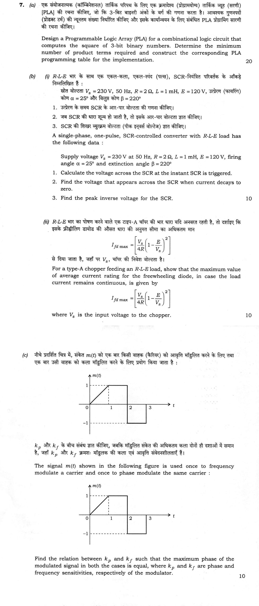
The signal m(t) shown in the following figure is used once to frequency modulate a carrier and once to phase modulate the same carrier :
Find the relation between k_p and k_f such that the maximum phase of the modulated signal in both the cases is equal, where k_p and k_f are phase and frequency sensitivities, respectively of the modulator. 10 marks
हिंदी में प्रश्न पढ़ें
एक संयोजनात्मक (कॉम्बिनेशनल) तार्किक परिपथ के लिए एक क्रमादेश्य (प्रोग्रामेयोग्य) तार्किक व्यूह (सरणी) [PLA] की रचना कीजिए, जो कि 3-बिट बाइनरी अंकों के वर्ग की गणना करता है। आवश्यक गुणनपदों (प्रोडक्ट टर्म) की न्यूनतम संख्या निर्धारित कीजिए और इसके कार्यान्वयन के लिए संबंधित PLA प्रोग्रामिंग सारणी की रचना कीजिए। (20 अंक)
R-L-E भार के साथ एक एकल-कला, एकल-स्पंद (पल्स), SCR-नियंत्रित परिवर्तक के आँकड़े निम्नलिखित हैं : स्रोत वोल्टता Vs = 230 V, 50 Hz, R = 2 Ω, L = 1 mH, E = 120 V, उत्तेजन (फायरिंग) कोण α = 25° और विलुप्त कोण β = 220° 1. उत्तेजन के समय SCR के आर-पार वोल्टता की गणना कीजिए। 2. जब SCR की धारा शून्य हो जाती है, तो इसके आर-पार वोल्टता ज्ञात कीजिए। 3. SCR की शिखर व्युत्क्रम वोल्टता (पीक इन्वर्स वोल्टेज) ज्ञात कीजिए। (10 अंक)
R-L-E भार का पोषण करने वाले एक टाइप-A चॉपर की भार धारा यदि अनवरत रहती है, तो दर्शाइए कि इसके फ्रीह्वीलिंग डायोड की औसत धारा की अनुमत सीमा का अधिकतम मान
Ifd max = [ Vs/4R (1 − E/Vs)² ]
से दिया जाता है, जहाँ पर Vs, चॉपर की निवेश वोल्टता है। (10 अंक)
निचे प्रदर्शित चित्र में, संकेत m(t) को एक बार किसी वाहक (कैरियर) को आवृत्ति मॉडुलित करने के लिए तथा एक बार उसी वाहक को कला मॉडुलित करने के लिए प्रयोग किया जाता है :
k_p और k_f के बीच संबंध ज्ञात कीजिए, जबकि मॉडुलित संकेत की अधिकतम कला दोनों ही दशाओं में समान है, जहाँ k_p और k_f क्रमशः मॉडूलक की कला एवं आवृत्ति संवेदनशीलताएँ हैं। (10 अंक)
Model answer
Drafted with AI by UPSC Answer Check against this question's marking rubric, to the expected length. UPSC does not publish answers for Mains — this is one way to score well, not an official key. How we build rubrics and answers.
(a) PLA to square a 3-bit binary number (20 marks)
Truth table. The input is A₂A₁A₀ (0 to 7) and the output is its square, at most 49, so six output bits B₅B₄B₃B₂B₁B₀ are needed.
- 000 (0) → 000000
- 001 (1) → 000001
- 010 (2) → 000100
- 011 (3) → 001001
- 100 (4) → 010000
- 101 (5) → 011001
- 110 (6) → 100100
- 111 (7) → 110001
Minimisation of each output (from the columns of the table):
- B₀ = 1 for 001, 011, 101, 111, so B₀ = A₀.
- B₁ = 0 for all inputs, so B₁ = 0 (its OR-plane line is left unconnected).
- B₂ = 1 for 010 and 110, so B₂ = A₁A₀′.
- B₃ = 1 for 011 and 101, so B₃ = A₂′A₁A₀ + A₂A₁′A₀ (= A₀(A₂ ⊕ A₁)); the two minterms cannot be combined.
- B₄ = 1 for 100, 101 and 111; the pairs (100, 101) and (101, 111) give B₄ = A₂A₁′ + A₂A₀.
- B₅ = 1 for 110 and 111, so B₅ = A₂A₁.
Minimum number of product terms. The distinct product terms are A₀, A₁A₀′, A₂′A₁A₀, A₂A₁′A₀, A₂A₁′, A₂A₀ and A₂A₁. No term is shared between outputs, and none can be removed, so the minimum is 7 product terms (6 if the output B₀ is wired directly from the input A₀ without using an AND-plane line).
PLA programming table (inputs: 1 = true, 0 = complemented, − = not connected; outputs: 1 = term connected to the OR gate of that output, − = not connected):
- P1: A₂ −, A₁ −, A₀ 1 → B₀ = 1
- P2: A₂ −, A₁ 1, A₀ 0 → B₂ = 1
- P3: A₂ 0, A₁ 1, A₀ 1 → B₃ = 1
- P4: A₂ 1, A₁ 0, A₀ 1 → B₃ = 1
- P5: A₂ 1, A₁ 0, A₀ − → B₄ = 1
- P6: A₂ 1, A₁ −, A₀ 1 → B₄ = 1
- P7: A₂ 1, A₁ 1, A₀ − → B₅ = 1
All other entries of the output columns (and the whole B₁ column) are unprogrammed. The PLA has 3 inputs, 7 product terms and 6 outputs (a 3 × 7 × 6 array, or 3 × 7 × 5 when the constant B₁ is dropped). Check: input 101 selects P1, P4, P5 and P6 and gives B₀ = 1, B₃ = 1, B₄ = 1, that is 011001 = 25.
(b)(i) Voltages across the SCR (10 marks)
The supply peak is V_m = 230√2 = 325.3 V. While the SCR is off the load current is zero, so the load voltage equals the back emf E and the SCR voltage is v_SCR = v_s − E = V_m sin ωt − E.
- At the instant of triggering, ωt = α = 25°. Just before firing, v_s = 325.3 sin 25° = 137.5 V, so v_SCR = 137.5 − 120 = 17.5 V (forward). Since 17.5 V > 0 the SCR is forward biased (α exceeds sin⁻¹(120/325.3) = 21.6°), and it drops to about 0 V once it conducts.
- When the current decays to zero, ωt = β = 220°. v_s = 325.3 sin 220° = −209.1 V, and the SCR is then reverse biased by v_SCR = −209.1 − 120 = −329.1 V.
- Peak inverse voltage. After extinction the SCR voltage is v_s − E, which is most negative when v_s = −V_m (ωt = 270°, which lies after β = 220°): PIV = V_m + E = 325.3 + 120 = 445.3 V.
(b)(ii) Maximum freewheeling-diode current of a type-A chopper (10 marks)
Model. A type-A (step-down) chopper with duty ratio δ = T_on/T applies V_s to the R–L–E load while the chopper is on and lets the load current freewheel through the diode while it is off. In continuous conduction, and assuming a small current ripple (the load current is essentially constant at its mean I_a), the output voltage is V_o = δV_s. The average voltage across L is zero, so
I_a = (δV_s − E)/R.
The diode carries the load current for the off-time (1 − δ)T, so its average current is
I_fd = (1 − δ) I_a = (1 − δ)(δV_s − E)/R.
Maximisation over δ. Differentiate:
dI_fd/dδ = (1/R)[−(δV_s − E) + (1 − δ)V_s] = (1/R)[V_s + E − 2δV_s] = 0, so δ = ½(1 + E/V_s).
The second derivative is −2V_s/R < 0, so this is a maximum. The value δ = ½(1 + E/V_s) lies between E/V_s and 1 for E ≤ V_s, so the load current is positive and the assumptions hold. At this δ:
- 1 − δ = ½(1 − E/V_s);
- δV_s − E = ½(V_s + E) − E = ½(V_s − E) = (V_s/2)(1 − E/V_s).
Therefore
I_fd,max = (1/R) × ½(1 − E/V_s) × (V_s/2)(1 − E/V_s) = (V_s/4R)(1 − E/V_s)²,
as required.
(c) Relation between k_p and k_f for equal maximum phase (10 marks)
The message is m(t) = t for 0 ≤ t ≤ 1, 1 for 1 ≤ t ≤ 2, −1 for 2 ≤ t ≤ 3, and 0 otherwise.
Phase modulation. The phase follows the message: φ_PM(t) = k_p m(t). Its maximum is k_p max|m(t)| = k_p × 1 = k_p.
Frequency modulation. The instantaneous frequency is f_i = f_c + k_f m(t), so the phase is the integral of the message:
φ_FM(t) = 2π k_f ∫₀ᵗ m(τ) dτ.
The integral is t²/2 for 0 ≤ t ≤ 1 (reaching 0.5), 0.5 + (t − 1) for 1 ≤ t ≤ 2 (reaching 1.5), 1.5 − (t − 2) for 2 ≤ t ≤ 3 (falling to 0.5), and stays at 0.5 afterwards. So max|∫m| = 1.5, at t = 2 s, and the maximum FM phase is 2π k_f × 1.5 = 3π k_f.

Condition. Equal maximum phase requires k_p = 3π k_f, that is k_p ≈ 9.42 k_f, with k_f in Hz per unit of m(t) and k_p in rad per unit of m(t). (If k_f were defined in rad/s per unit, φ_FM = k_f ∫m and the condition would be k_p = 1.5 k_f.)
How this answer will be evaluated
Evaluation rubric
Each sub-part is marked on its own, against the marks and word limit printed on the paper.
- (a) Design a PLA that squares a 3-bit binary number: truth table, minimised output expressions, minimum number of product terms and the PLA programming table. 20 marks
Must cover
- Squares 0, 1, 4, 9, 16, 25, 36, 49 need six output bits
- B₀ = A₀, B₁ = 0, B₂ = A₁A₀′, B₃ = A₂′A₁A₀ + A₂A₁′A₀, B₄ = A₂A₁′ + A₂A₀, B₅ = A₂A₁
- Minimum of 7 distinct product terms
- Programming table for the AND plane (3 inputs, 7 terms) and OR plane (6 outputs), a 3 × 7 × 6 PLA
Loses marks
- Using 8 outputs or 3 output bits.
- Giving a ROM-style 8-minterm table instead of a minimised PLA.
- Sharing terms incorrectly so that a square is wrong.
Earns more
- Truth table with all eight rows.
- Verification of one input, such as 101 giving 25.
Extra mark
- Note that B₀ can be wired directly, reducing the count to 6, and B₁ needs no term
- (b)(i) For a single-phase half-wave SCR converter with R-L-E load (230 V, 50 Hz, R = 2 Ω, L = 1 mH, E = 120 V, α = 25°, β = 220°) find the SCR voltage at triggering, at current zero, and the peak inverse voltage. 10 marks
Must cover
- V_m = 325.3 V and v_SCR = v_s − E while the SCR is blocking
- +17.5 V at α = 25°
- −329 V at β = 220°
- PIV = V_m + E = 445 V
Loses marks
- Taking v_SCR = v_s without subtracting E.
- Using PIV = V_m = 325 V.
- Using an RMS instead of peak supply value.
Earns more
- Reason for the PIV: v_s reaches −V_m at 270°, after extinction.
- Check that the SCR is forward biased at α (α > 21.6°).
Extra mark
- Note that the SCR voltage falls to about 0 V after firing
- (b)(ii) Prove that for a type-A chopper feeding an R-L-E load in continuous conduction the maximum average freewheeling-diode current is (V_s/4R)(1 − E/V_s)². 10 marks
Must cover
- V_o = δV_s and I_a = (δV_s − E)/R for continuous conduction
- Diode conducts for (1 − δ)T, so I_fd = (1 − δ)I_a
- Differentiation gives δ_opt = ½(1 + E/V_s), with a second-derivative check
- Substitution gives I_fd,max = (V_s/4R)(1 − E/V_s)²
Loses marks
- Quoting the result with no derivation.
- Using I_fd = δ I_a.
- Optimising over E or R instead of the duty ratio.
Earns more
- Statement of the ripple-free assumption.
- Check that δ_opt lies in the valid range.
Extra mark
- Physical interpretation: the diode current is largest when the switch and diode share the period roughly equally
- (c) Find the relation between k_p and k_f so that the maximum phase of the modulated signal is equal for PM and FM with the given m(t). 10 marks
Must cover
- PM phase k_p m(t), maximum k_p × 1
- FM phase 2πk_f ∫m dt
- max|∫m| = 1.5 at t = 2 s, so maximum FM phase 3πk_f
- k_p = 3πk_f ≈ 9.42 k_f
Loses marks
- Using the maximum of m(t) for both PM and FM.
- Omitting the 2π factor in the FM phase.
- Taking the maximum of the integral as 1 or 2.
Earns more
- Piecewise integral worked out over each interval.
- Statement of the sensitivity convention (k_f in Hz per unit).
Extra mark
- Sketch of the integral of m(t) showing the peak at t = 2 s
What "Construct" is asking you to do
Build the required object — a velocity diagram, a sequential test, a control chart, a geometrical figure — step by step, so the sequence is visible on the page. The steps are marked, not only the finished thing.
Structure that answers it
Data and requirement → scale or basis chosen, stated → construction steps in order → the finished construction, labelled → quantities read off, or the result it yields
Where marks are lost
A diagram drawn without a stated scale, so nothing can be scaled off it and the quantities that follow lose their support. In statistics, writing down the procedure without fixing its defining constants — stopping bounds in terms of the two error probabilities, or the control limits — leaves it unmarkable.
Practice this exact question
Write your answer and it is marked point by point against the model answer above — what you covered, what you missed, what you got wrong.
Evaluate my answer →More from Electrical Engineering 2026 Paper I
- Q4 (a) (i) The continuous-time signal x(t) = cos(20πt + π/4) is ideally sampled at a rate of…
- Q5 (a) For the circuit given in the figure below, the input voltage signal is given by V_in…
- Q6 (a) Design a MOD-6 synchronous DOWN counter using J-K flip-flops. (20 marks) (b) A three-…
- Q7 (a) Design a Programmable Logic Array (PLA) for a combinational logic circuit that comput…
- Q8 (a) A 6·6 kV, three-phase, star-connected, cylindrical-rotor alternator develops rated vo…