Paper II — Q5
(a) Show that the energy of the triplet state (S = 1) is not equal to the energy of the singlet state (S = 0). 10 marks (b) ρ⁰…
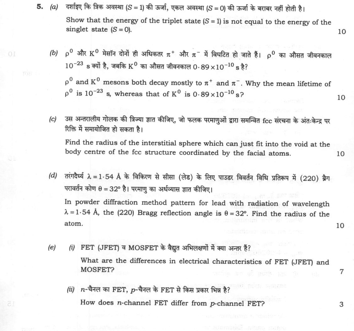
Show that the energy of the triplet state (S = 1) is not equal to the energy of the singlet state (S = 0). 10 marks
ρ⁰ and K⁰ mesons both decay mostly to π⁺ and π⁻. Why the mean lifetime of ρ⁰ is 10⁻²³ s, whereas that of K⁰ is 0·89 × 10⁻¹⁰ s? 10 marks
Find the radius of the interstitial sphere which can just fit into the void at the body centre of the fcc structure coordinated by the facial atoms. 10 marks
In powder diffraction method pattern for lead with radiation of wavelength λ = 1·54 Å, the (220) Bragg reflection angle is θ = 32°. Find the radius of the atom. 10 marks
What are the differences in electrical characteristics of FET (JFET) and MOSFET? 7 marks
How does n-channel FET differ from p-channel FET? 3 marks
हिंदी में प्रश्न पढ़ें
दर्शाइए कि त्रिक अवस्था (S = 1) की ऊर्जा, एकल अवस्था (S = 0) की ऊर्जा के बराबर नहीं होती है। 10
ρ⁰ और K⁰ मेसॉन दोनों ही अधिकतर π⁺ और π⁻ में विघटित हो जाते हैं। ρ⁰ का औसत जीवनकाल 10⁻²³ s क्यों है, जबकि K⁰ का औसत जीवनकाल 0·89 × 10⁻¹⁰ s है? 10 marks
उस अंतरालीय गोलक की त्रिज्या ज्ञात कीजिए, जो फलक परमाणुओं द्वारा समन्वित fcc संरचना के अंतःकेंद्र पर रिक्ति में समायोजित हो सकता है। 10
तरंगदैर्ध्य λ = 1·54 Å के विकिरण से सीसा (लेड) के लिए पाउडर विवर्तन विधि प्रतिरूप में (220) श्रेण परावर्तन कोण θ = 32° है। परमाणु का अर्धव्यास ज्ञात कीजिए। 10
FET (JFET) व MOSFET के वैद्युत अभिलक्षणों में क्या अंतर हैं? 7 marks
n-चैनल का FET, p-चैनल के FET से किस प्रकार भिन्न है? 3 marks
Model answer
Written by UPSC Answer Check against this question's marking rubric, to the expected length. UPSC does not publish answers for Mains — this is one way to score well, not an official key.
(a) For a two-electron atom or excited configuration with two distinct one-electron orbitals φ₁ and φ₂, the total wavefunction must be antisymmetric under exchange of the two electrons. The singlet state S = 0 has antisymmetric spin function, so its spatial part must be symmetric: ψₛ = (1/√2)[φ₁(r₁)φ₂(r₂) + φ₁(r₂)φ₂(r₁)]. The triplet state S = 1 has symmetric spin function, so its spatial part must be antisymmetric: ψₜ = (1/√2)[φ₁(r₁)φ₂(r₂) − φ₁(r₂)φ₂(r₁)].
Take the two-electron Hamiltonian H = h₁ + h₂ + e²/(4πε₀ r₁₂). Define the direct Coulomb integral J = ∫∫ |φ₁(r₁)|² |φ₂(r₂)|² e²/(4πε₀ r₁₂) dr₁ dr₂ and the exchange integral K = ∫∫ φ₁*(r₁)φ₂*(r₂) e²/(4πε₀ r₁₂) φ₂(r₁)φ₁(r₂) dr₁ dr₂.
Using the above spatial functions: Eₛ = ⟨ψₛ|H|ψₛ⟩ = E₁ + E₂ + J + K, Eₜ = ⟨ψₜ|H|ψₜ⟩ = E₁ + E₂ + J − K. Therefore Eₛ − Eₜ = 2K. For overlapping atomic orbitals and repulsive electron-electron interaction, K ≠ 0 and is usually positive. Hence the singlet and triplet energies are not equal; the splitting is the exchange splitting. This requires the two electrons to occupy different spatial orbitals. If both electrons occupy the same spatial orbital, the antisymmetric triplet spatial function vanishes, so only the singlet state can exist.
(b) Both ρ⁰ and K⁰ can be observed in the π⁺π⁻ channel, but their decay mechanisms are different.
ρ⁰ is a quark-antiquark resonance, e.g. (uū − dd̄)/√2, with zero strangeness. The decay ρ⁰ → π⁺ + π⁻ conserves strangeness and can proceed through the strong interaction. Strong decays have widths of order 100 MeV. For ρ⁰, Γ ≈ 150 MeV, so τ = ħ/Γ ≈ (6·58 × 10⁻²² MeV s)/(150 MeV) ≈ 4 × 10⁻²⁴ s, which is conventionally quoted as of order 10⁻²³ s, the strong-interaction timescale.
K⁰ has strangeness S = +1. The final pions have S = 0, so the decay requires ΔS = 1. Strong and electromagnetic interactions conserve strangeness, so K⁰ cannot decay strongly or electromagnetically to π⁺π⁻. It must decay through the weak interaction, which is much weaker. The 0·89 × 10⁻¹⁰ s value is essentially the lifetime of the short-lived neutral kaon component K_S. Its weak width is Γ ≈ ħ/τ ≈ (6·58 × 10⁻²² MeV s)/(0·89 × 10⁻¹⁰ s) ≈ 7·4 × 10⁻¹² MeV, which is about 10¹³ times smaller than the ρ⁰ width. Thus the huge lifetime difference is due to strong decay for ρ⁰ and strangeness-changing weak decay for K⁰.
(c) In fcc, the body centre is an octahedral interstitial void coordinated by six face-centred atoms. Let the lattice constant be a and the atomic radius be R.
For fcc atoms touching along a face diagonal: 4R = √2 a, so R = a/(2√2).
The body centre is at (a/2, a/2, a/2). A nearest face-centred atom is, for example, at (a/2, a/2, 0). The distance from the body centre to this face-centred atom is d = a/2.
Let r be the radius of the interstitial sphere that just fits. It touches the six face-centred atoms, so d = R + r. Hence r = a/2 − R = a/2 − a/(2√2) = (a/2)(1 − 1/√2).
Using a = 2√2 R: r = √2 R − R = (√2 − 1)R. Therefore r = (√2 − 1)R ≈ 0·414R. Equivalently, r/a = (√2 − 1)/(2√2) ≈ 0·1464. This is the octahedral void radius in fcc.
(d) Lead has an fcc structure. For a cubic crystal, the interplanar spacing for (hkl) is dₕₖₗ = a/√(h² + k² + l²). For (220), h² + k² + l² = 2² + 2² + 0² = 8, so d₂₂₀ = a/√8 = a/(2√2).
For fcc, atoms touch along the face diagonal: 4R = √2 a, so R = a/(2√2). Thus d₂₂₀ = R.
Using Bragg’s law for first order, n = 1: λ = 2 d₂₂₀ sinθ = 2R sinθ. Therefore R = λ/(2 sinθ).
Put λ = 1·54 Å and θ = 32°: sin32° = 0·5299. R = 1·54/(2 × 0·5299) = 1·54/1·0598 = 1·453 Å. R ≈ 1·45 Å. The corresponding lattice constant is a = 2√2 R ≈ 4·11 Å.
(e)(i) Differences in electrical characteristics of JFET and MOSFET:
- Gate structure: JFET uses a reverse-biased p-n junction gate. MOSFET uses an insulated gate separated by a thin oxide layer.
- Gate current and input resistance: JFET has very small but finite gate leakage current; input resistance is high, typically about 10⁸–10¹⁰ Ω. MOSFET gate leakage is extremely small through the oxide, so input resistance is much higher, often 10¹²–10¹⁵ Ω.
- Control mechanism: JFET controls current by varying the depletion-layer width in the channel. MOSFET controls current by field-induced inversion or depletion of the channel.
- Operating mode: JFET operates only in depletion mode and is normally ON. MOSFET can be enhancement type or depletion type; the common enhancement MOSFET is normally OFF.
- Transfer characteristic: For an n-channel JFET, I_D = I_DSS(1 − V_GS/V_P)². For an enhancement n-channel MOSFET, I_D = k(V_GS − V_T)² for V_GS > V_T.
- Capacitance and noise: MOSFETs usually have higher input capacitance and greater flicker noise due to oxide traps. JFETs often have lower noise.
- Ruggedness: MOSFET gate oxide can be damaged by electrostatic discharge. JFET is relatively more robust.
- Terminals: JFET is normally a three-terminal device. MOSFET often has a fourth body/substrate terminal, giving rise to the body effect.
(e)(ii) In an n-channel FET, current is carried by electrons; in a p-channel FET, current is carried by holes. An n-channel MOSFET conducts when V_GS is more positive than the threshold voltage, with drain positive with respect to source. A p-channel MOSFET conducts when V_GS is more negative than the threshold voltage, with drain negative with respect to source. For JFETs, an n-channel JFET requires a negative gate-to-source voltage, while a p-channel JFET requires a positive gate-to-source voltage. Since electron mobility is higher than hole mobility, an n-channel FET usually has higher transconductance, lower ON resistance, and faster switching than a comparable p-channel FET.
What "Derive" is asking you to do
Reach the stated expression from a starting relation, justifying every step. The destination is printed in the question, so only the route earns marks, and the assumptions you work under are part of that route.
Structure that answers it
Assumptions and notation defined → starting relation or governing equation → each step with its justification → the required expression → limiting case or boundary check
Where marks are lost
Writing the standard result first and fitting three lines to it, which an examiner reads at a glance. Marks also go on assumptions left unstated — lossless medium, small amplitude, errors independent with zero mean — and on symbols used before they are defined, even when the question says usual notations.
How this answer will be evaluated
Approach
(a) derive: given > assumptions > stepwise derivation > result > check | (b) explain: definition/context > points in order > small example > short close | (c) calculate: given > formula > substitution > result with units > interpretation | (d) calculate: given > formula > substitution > result with units > interpretation | (e(i)) compare: paired headings or table > key differences > significance > conclusion | (e(ii)) explain: definition/context > points in order > small example > short close Full marks: All parts show full derivation, correct physics, units, and physical interpretation.
Key points expected
- Write total spin S and multiplicity 2S+1
- State exchange interaction or spin-spin coupling
- Show E(S=1) ≠ E(S=0) via energy term
- Identify which state is lower energy
- Identify decay modes (strong vs weak)
- State ρ⁰ decays via strong interaction
- State K⁰ decays via weak interaction
- Link interaction type to lifetime scale
Evaluation rubric
Each sub-part is marked on its own, against the marks and word limit printed on the paper.
- (a) Derive energy difference between triplet and singlet states. 10 marks
derive— given → assumptions → stepwise derivation → result → check
Must cover
- Write total spin S and multiplicity 2S+1
- State exchange interaction or spin-spin coupling
- Show E(S=1) ≠ E(S=0) via energy term
- Identify which state is lower energy
Loses marks
- No derivation, just assertion
- Confusing spin with orbital angular momentum
- Missing units or dimension check
Earns more
- Mention Hund's rule
- Relate to Pauli exclusion principle
- Give example (e.g., helium or carbon)
Extra mark
- Draw energy level diagram
- Mention fine structure constant
- (b) Explain lifetime difference between ρ⁰ and K⁰ mesons. 10 marks
explain— definition/context → points in order → small example → short close
Must cover
- Identify decay modes (strong vs weak)
- State ρ⁰ decays via strong interaction
- State K⁰ decays via weak interaction
- Link interaction type to lifetime scale
Loses marks
- No mention of interaction type
- Confusing ρ⁰ with π⁰
- No physical reasoning, just numbers
Earns more
- Mention quark content (uū vs d s̄)
- Cite typical strong/weak timescales
- Note branching ratios
Extra mark
- Draw Feynman diagrams for both decays
- Mention CP violation in K⁰ system
- (c) Calculate radius of interstitial sphere in fcc body-centre void. 10 marks
calculate— given → formula → substitution → result with units → interpretation
Must cover
- Define fcc lattice parameter a and atomic radius R
- State body-centre void is coordinated by 8 face atoms
- Use geometry: distance from body centre to face centre = (√3/2)a
- Set r + R = (√3/2)a and solve for r/R
Loses marks
- Wrong coordination number (e.g., 6 instead of 8)
- No geometric derivation
- Missing units or dimension check
Earns more
- Show diagram of fcc unit cell with void
- State R = a√2/4 for fcc
- Give final ratio r/R ≈ 0.225
Extra mark
- Compare with octahedral void size
- Mention real materials using this void
- (d) Find atomic radius of lead from Bragg diffraction data. 10 marks
calculate— given → formula → substitution → result with units → interpretation
Must cover
- Use Bragg’s law: nλ = 2d sinθ
- Relate d₂₂₀ to lattice parameter a: d = a/√(h²+k²+l²)
- Substitute h=2,k=2,l=0 → d = a/√8
- Solve for a, then use fcc relation R = a√2/4
Loses marks
- Wrong d-spacing formula
- No unit conversion (Å to m or vice versa)
- Skipping derivation of R from a
Earns more
- Show step-by-step substitution with units
- State assumption: lead is fcc
- Check dimensional consistency
Extra mark
- Compare with known atomic radius of Pb
- Mention powder diffraction pattern indexing
- (e(i)) Compare electrical characteristics of JFET and MOSFET. 7 marks
compare— paired headings or table → key differences → significance → conclusion
Must cover
- List key differences: gate structure, input impedance, control mechanism
- JFET: reverse-biased p-n junction; MOSFET: insulated gate
- MOSFET has higher input impedance
- JFET is unipolar, MOSFET can be enhancement/depletion
Loses marks
- No distinction between gate types
- Confusing JFET with BJT
- Missing key parameter like input impedance
Earns more
- Mention threshold voltage vs pinch-off voltage
- Note MOSFET is voltage-controlled, JFET also but with different mechanism
- Include symbol or equivalent circuit
Extra mark
- Table format for comparison
- Mention applications (e.g., MOSFET in digital, JFET in analog)
- (e(ii)) Explain difference between n-channel and p-channel FET. 3 marks
explain— definition/context → points in order → small example → short close
Must cover
- n-channel: majority carriers are electrons
- p-channel: majority carriers are holes
- Source/drain and gate polarity reversed
- Voltage polarity for conduction differs
Loses marks
- No mention of carrier type
- Confusing n-channel with n-type substrate
- Missing voltage polarity difference
Earns more
- Mention symbol difference (arrow direction)
- Note typical use in CMOS (complementary pair)
Extra mark
- Draw symbols for both
- Mention mobility difference (electrons > holes)
Practice this exact question
Write your answer and it is marked point by point against the model answer above — what you covered, what you missed, what you got wrong.
Evaluate my answer →More from Physics 2025 Paper II
- Q2 (a) What is the density of states? For a relativistic particle of rest mass μ, prove that…
- Q3 (a) Find out the difference in frequencies of Lyman-alpha line in hydrogen and deuterium…
- Q4 (a) State how for spin-half particles, the spin (σ) can be expressed by its three compone…
- Q5 (a) Show that the energy of the triplet state (S = 1) is not equal to the energy of the s…
- Q6 (a) The total binding energies of ¹⁵₈O, ¹⁶₈O and ¹⁷₈O are 111·96 MeV, 127·62 MeV and 131·…
- Q7 (a) What is the minimum energy required to break a ₂He⁴ nucleus into free protons and neu…
- Q8 (a) Classify diamagnetic, paramagnetic and ferromagnetic materials in terms of their magn…