Paper I — Q1
(a) For the circuit shown in Figure 1(a), find the V_in, V_S and power supplied by the dependent source. (10 marks) (b) Calculate…
For the circuit shown in Figure 1(a), find the V_in, V_S and power supplied by the dependent source. 10 marks
Calculate the forward current caused by 0·8 V forward voltage across the diode with ideality factor of semiconductor material as 1. The reverse saturation current of diode is 12·674 × 10⁻¹³ A at a temperature of 22°C. [Assume Boltzmann constant K = 1·38 × 10⁻²³ JK⁻¹, charge of electron q = 1·6 × 10⁻¹⁹ C] 10 marks
Find the efficiency of a long shunt compound generator rated at 250 kW, 230 V when supplying 75% rated load at rated voltage. The resistances of armature and series field are 0·009 Ω and 0·003 Ω respectively. The shunt field current is 13 A. When the machine is running as a motor at no-load, the armature current is 25 A at rated voltage. 10 marks
An op-amp circuit is shown in Figure 1(d) below. Assume the op-amp to be ideal. (i) Determine I_1, I_2, I_3 and V_X. (ii) If V_0 is not to be lower than −13 V, calculate the maximum allowed value for R_L. (iii) If R_L is varied in the range 100 Ω to 1 kΩ, what is the corresponding change in I_L and in V_0? 10 marks
Explain the parity bit generator and parity bit checker. Realize the even parity bit generator and even parity bit checker using X-OR gate. 10 marks
हिंदी में प्रश्न पढ़ें
चित्र 1(a) में दर्शाए गए परिपथ के लिए V_in, V_S और आश्रित स्रोत द्वारा आपूर्ति की गई शक्ति के मान ज्ञात कीजिए। (10 अंक)
तत्समक गुणांक 1 (एक) वाले अर्धचालक पदार्थ के डायोड के आर-पार 0·8 V अग्र बोल्टता के कारण उत्पन्न अग्र धारा का मान परिकलित कीजिए। 22°C तापमान पर डायोड की उत्क्रम संतृप्ति धारा 12·674 × 10⁻¹³ A है। [बोल्ट्ज़मान स्थिरांक K = 1·38 × 10⁻²³ JK⁻¹, इलेक्ट्रॉन का आवेश q = 1·6 × 10⁻¹⁹ C मान लीजिए] (10 अंक)
निर्धारित बोल्टता पर 75% निर्धारित भार की आपूर्ति करते समय 250 kW, 230 V द्वारा निर्धारित मान के एक दीर्घ पार्श्व पथ मिश्र कुंडलित जनित्र की दक्षता ज्ञात कीजिए। आर्मेचर एवं श्रेणी क्षेत्र के प्रतिरोध क्रमशः: 0·009 Ω और 0·003 Ω हैं। पार्श्व (शंट) क्षेत्र की धारा 13 A है। यह मशीन जब बिना किसी भार की मोटर की तरह कार्य करती है तो निर्धारित बोल्टता पर आर्मेचर की धारा 25 A है। (10 अंक)
चित्र 1(d) में संक्रियात्मक-प्रवर्धक (op-amp) परिपथ को नीचे दर्शाया गया है। संक्रियात्मक-प्रवर्धक (op-amp) को आदर्श मान लीजिए। (i) I₁, I₂, I₃ और Vₓ के मान ज्ञात कीजिए। (ii) Rₗ के अधिकतम अनुमत मान की गणना कीजिए, जबकि V₀ का मान −13 V से कम न हो। (iii) यदि R_L का मान 100 Ω से 1 kΩ की सीमा में परिवर्तित होता है, तो तदनुसार V_0 तथा I_L में क्या परिवर्तन होगा? (10 अंक)
पैरिटी बिट जनित्र व पैरिटी बिट परीक्षक की व्याख्या कीजिए। सम-पैरिटी बिट जनित्र व सम-पैरिटी बिट परीक्षक को X-OR गेट के प्रयोग द्वारा साकार कीजिए। (10 अंक)
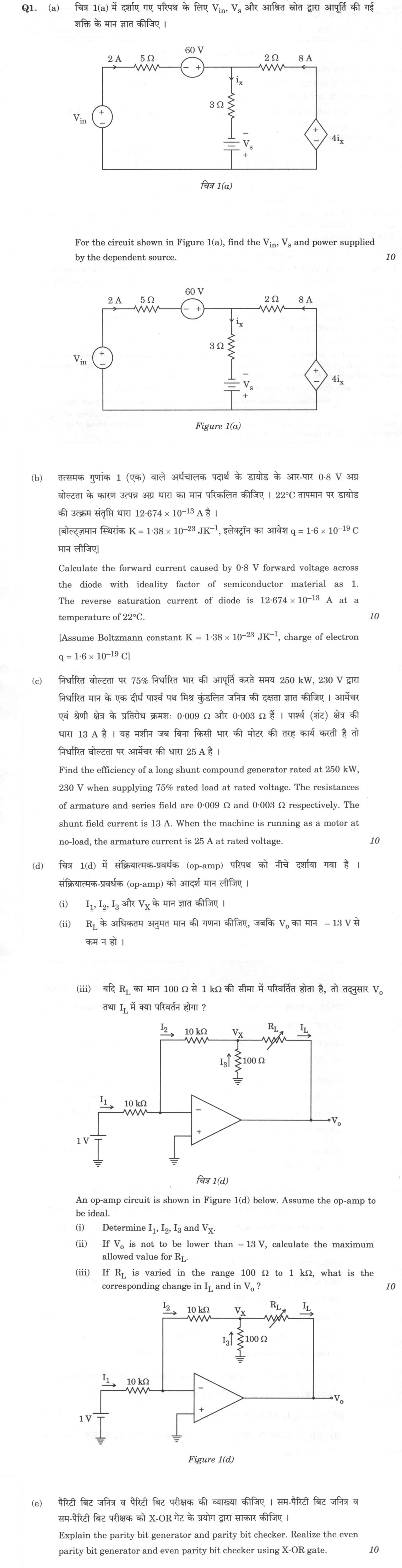
The figure this question refers to, in words
The question paper is a scan and the diagram did not survive as text. This is the figure as read from the original page — every component, value and label — so the question can be worked from the text below.
(a) Circuit diagram labeled Figure 1(a). The circuit consists of three parallel vertical branches connected by top and bottom horizontal wires. The bottom wire is a common ground rail. The left branch contains a voltage source labeled Vin with its positive terminal at the top and negative terminal at the bottom. The middle branch contains a 3 Ohm resistor in series with a voltage source labeled Vs. The positive terminal of Vs is at the bottom and the negative terminal is at the top. The current flowing down through this branch is labeled ix. The right branch contains a dependent voltage source labeled 4ix with its positive terminal at the top and negative terminal at the bottom. The top horizontal wire connects the top of the left branch to the top of the middle branch via a series combination of a 5 Ohm resistor and a 60 V voltage source. The 60 V source has its negative terminal on the left and positive terminal on the right. The current flowing from left to right in this section is labeled 2 A. The top of the middle branch connects to the top of the right branch via a 2 Ohm resistor. The current flowing from right to left in this section is labeled 8 A.
(d) Circuit diagram labeled Figure 1(d). An ideal operational amplifier (op-amp) is shown with an inverting input (-) and a non-inverting input (+). The non-inverting input is connected to ground. A 1 V DC voltage source is connected to ground at one end and to a 10 kΩ resistor at the other end. The other end of this 10 kΩ resistor is connected to the inverting input of the op-amp. The current flowing from the 1 V source through this resistor is labeled I1. The inverting input node is also connected to a 10 kΩ resistor. The current flowing from the inverting input node through this second 10 kΩ resistor is labeled I2. The other end of this second 10 kΩ resistor is connected to a node labeled Vx. From node Vx, a 100 Ω resistor is connected to ground, with the current flowing from Vx to ground labeled I3. Also from node Vx, a variable resistor labeled RL is connected to the output terminal of the op-amp. The current flowing from node Vx through RL to the output is labeled IL. The output terminal of the op-amp is labeled V0.
What "Solve" is asking you to do
Choose the method, then carry it through to a final answer. Identifying what kind of problem this is and why that method applies is the first thing marked; a correct figure arrived at invisibly earns almost nothing.
Structure that answers it
Given data and what is required → method chosen, with the reason it applies → set-up (equation, circuit, free body, trial balance) → working, step by step → answer with units and any condition of validity
Where marks are lost
Doing the middle steps mentally and writing only the result. In mathematics papers, a further loss comes from giving a decimal where the exact value in surds or fractions was wanted, or from skipping the justification a part explicitly asks for.
How this answer will be evaluated
Approach
(a) calculate: given > formula > substitution > result with units > interpretation | (b) calculate: given > formula > substitution > result with units > interpretation | (c) calculate: given > formula > substitution > result with units > interpretation | (d) calculate: given > formula > substitution > result with units > interpretation | (e) explain: definition/context > points in order > small example > short close Full marks: Systematic application of circuit laws and formulas with clear steps and correct units.
Key points expected
- Apply KCL at the central node to find i_x
- Apply KVL to the left loop to find V_in
- Apply KVL to the middle branch to find V_s
- Calculate power using P = V * I with correct sign
- State the diode current equation I = I_s(e^(V/VT) - 1)
- Calculate thermal voltage V_T = kT/q
- Substitute given values for V, I_s, and V_T
- Provide final current value with units
Evaluation rubric
Each sub-part is marked on its own, against the marks and word limit printed on the paper.
- (a) Determine V_in, V_s, and power supplied by the dependent source. 10 marks
calculate— given → formula → substitution → result with units → interpretation
Must cover
- Apply KCL at the central node to find i_x
- Apply KVL to the left loop to find V_in
- Apply KVL to the middle branch to find V_s
- Calculate power using P = V * I with correct sign
Loses marks
- Sign error in KVL loop equations
- Incorrect calculation of i_x from KCL
Earns more
- Correctly identifies the dependent source value 4i_x
- Explicitly states reference directions for currents and voltages
Extra mark
- Verifies power balance for the entire circuit
- (b) Calculate the forward current of the diode. 10 marks
calculate— given → formula → substitution → result with units → interpretation
Must cover
- State the diode current equation I = I_s(e^(V/VT) - 1)
- Calculate thermal voltage V_T = kT/q
- Substitute given values for V, I_s, and V_T
- Provide final current value with units
Loses marks
- Using Celsius temperature directly in V_T calculation
- Omitting the -1 term in the diode equation
Earns more
- Correct conversion of temperature to Kelvin (295 K)
- Accurate calculation of the exponential term
Extra mark
- Mention of ideality factor n=1 explicitly in the formula
- (c) Find the efficiency of the long shunt compound generator. 10 marks
calculate— given → formula → substitution → result with units → interpretation
Must cover
- Calculate load current and armature current at 75% load
- Compute copper losses (armature, series, shunt)
- Determine iron and mechanical losses from no-load data
- Calculate efficiency as Output / (Output + Total Losses)
Loses marks
- Incorrect calculation of armature current (I_a = I_L + I_sh)
- Ignoring the series field resistance in loss calculation
Earns more
- Correct identification of no-load current as iron/mech loss component
- Clear separation of shunt and series field currents
Extra mark
- Tabulation of all individual loss components
- (d) Determine currents, voltages, and limits for the op-amp circuit. 10 marks
calculate— given → formula → substitution → result with units → interpretation
Must cover
- Apply virtual ground concept (V- = 0) for ideal op-amp
- Calculate I_1, I_2, I_3 using Ohm's law and KCL
- Determine V_X based on node voltage at the inverting input
- Calculate max R_L using the -13V saturation limit
Loses marks
- Assuming current flows into the op-amp input terminals
- Incorrect sign for V_0 or I_L
Earns more
- Correct application of KCL at the inverting node
- Accurate calculation of V_0 for the R_L range in part (iii)
Extra mark
- Explicit statement of the virtual short assumption
- (e) Explain parity generator/checker and realize even parity using X-OR. 10 marks
explain— definition/context → points in order → small example → short close
Must cover
- Define parity bit generator and checker functions
- Explain the logic of even parity (sum of bits = 0)
- Show X-OR gate realization for the generator
- Show X-OR gate realization for the checker
Loses marks
- Confusing even and odd parity logic
- Missing the feedback or comparison step in the checker
Earns more
- Clear distinction between generator and checker logic
- Correct labeling of inputs and outputs in the logic diagrams
Extra mark
- Truth table for the X-OR based parity logic
Model answer coming soon
Every evaluation on this site is marked against a verified model answer. This question's answer is still being written; evaluation opens the moment it lands.
More from Electrical Engineering 2022 Paper I
- Q1 (a) For the circuit shown in Figure 1(a), find the V_in, V_S and power supplied by the de…
- Q2 (a) (i) For the circuit shown in Figure 2(a)(i), initial current through the coil is zero…
- Q3 A common-emitter amplifier circuit is shown in Figure 3(a). Neglect r_x and r_o and assum…
- Q4 For the network shown in Figure 4(a)(i) and its excitation function shown in Figure 4(a)(…