Paper I — Q6
(a) The plane wave E = 30 cos (ωt – z) aₓ V/m in air normally hits a lossless medium (μ = μ₀, ε = 4ε₀) at z = 0. (i) Find…
The plane wave E = 30 cos (ωt – z) aₓ V/m in air normally hits a lossless medium (μ = μ₀, ε = 4ε₀) at z = 0. (i) Find reflection coefficient (Γ), transmission coefficient (τ), standing wave ratio (S). (ii) Calculate the reflected electric and magnetic fields. 20 marks
Determine the value of inductance L, capacitance C and duty cycle of a buck regulator shown in Figure 6(b). The input voltage is 16 V, output voltage is 4 V, and ripple voltage (peak-to-peak) is 30 mV. The regulator is operating at 20 kHz switching frequency and peak-to-peak ripple current in inductance is 0·75 A. 20 marks
Using the superposition theorem find the voltage 'V' across the 5 Ω resistance in the circuit as shown in Figure 6(c). 10 marks
हिंदी में प्रश्न पढ़ें
वायु में एक समतल तरंग E = 30 cos (ωt – z) aₓ V/m एक क्षयहीन माध्यम (μ = μ₀, ε = 4ε₀) से लम्बवत् z = 0 पर टकराती है । (i) परावर्तन गुणांक (Γ), संचरण गुणांक (τ) व अप्रगामी तरंग अनुपात (S) का मान ज्ञात कीजिए । (ii) परावर्तित विद्युत-क्षेत्र व चुंबकीय क्षेत्र की गणना कीजिए । 20 अंक
चित्र 6(b) में दर्शाए गए प्रतिकारी नियंत्रक (बक रेगुलेटर) के लिए प्रेरकत्व L, धारिता C व उपयोगिता अनुपात का मान निर्धारण कीजिए । परिपथ की निवेश वोल्टता 16 V, निर्गम वोल्टता 4 V, व ऊर्मिका वोल्टता (चरमांतर) 30 mV है । नियामक (रेगुलेटर) का प्रचालन 20 kHz स्विचिंग आवृत्ति पर होता है व प्रेरकत्व में चरमांतर ऊर्मिका धारा का मान 0·75 A है । 20 अंक
चित्र 6(c) में दर्शाए गए परिपथ में अध्यारोपण प्रमेय की सहायता से 5 Ω प्रतिरोध पर वोल्टता 'V' का मान ज्ञात कीजिए । 10 अंक
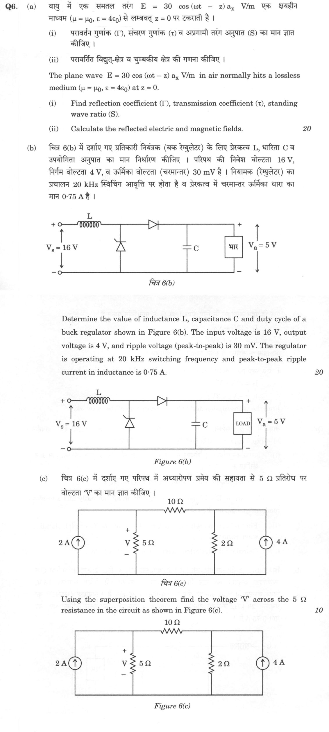
The figure this question refers to, in words
The question paper is a scan and the diagram did not survive as text. This is the figure as read from the original page — every component, value and label — so the question can be worked from the text below.
(b) Circuit diagram of a DC-DC converter labeled 'चित्र 6(b)': A DC input voltage source is connected at the left terminals with an upward arrow labeled Vs = 16 V, with the top terminal marked '+' and bottom terminal marked '-'. The top terminal connects to an inductor labeled L in the upper line. After the inductor, at an intermediate node, a thyristor (SCR) is connected in a vertical branch to the bottom rail, with its anode at the intermediate node, cathode at the bottom rail, and a gate terminal shown. A diode is connected in series in the upper line with its anode at the intermediate node and cathode directed toward the output. Across the output rails (after the diode), a capacitor C is connected in parallel, followed by a load block labeled 'भार' (Load) in parallel. At the far right output terminals, an upward arrow indicates the output voltage labeled Va = 5 V, with the top terminal marked '+' and bottom terminal marked '-'.
(b) Circuit diagram labeled Figure 6(b): A DC voltage source Vs = 16 V is connected at the input terminals (+ at top, - at bottom, with an upward arrow). From the positive terminal, an inductor L is connected in series along the top rail. Following the inductor, a controllable semiconductor switch (drawn as a thyristor/switch) is connected in a shunt branch directed downward to the bottom negative rail. In the top rail following this node is a series diode with its anode to the inductor and cathode to the right. After the diode, a capacitor C is connected in parallel between the top and bottom rails, followed by a parallel block labeled LOAD. Across the load, the output voltage is indicated as Va = 5 V with an upward arrow (+ at top, - at bottom).
(c) Circuit diagram labeled Figure 6(c): A two-mesh network consisting of a common continuous bottom reference wire and a segmented top rail. On the left side, between the top-left node and the bottom rail, are connected in parallel: an independent current source of 2 A directed upwards, and a 5 Omega resistor across which a voltage V is defined (+ at the top terminal, - at the bottom terminal). A 10 Omega resistor is connected horizontally along the top rail between the top-left node and the top-right node. On the right side, between the top-right node and the bottom rail, are connected in parallel: a 2 Omega resistor, and an independent current source of 4 A directed upwards.
Model answer
Written by UPSC Answer Check against this question's marking rubric, to the expected length. UPSC does not publish answers for Mains — this is one way to score well, not an official key.
(a)(i) For normal incidence, the wave impedance of medium 1 (air) is η₁ = √(μ₀/ε₀) = η₀ = 120π Ω ≈ 377 Ω. For medium 2, μ₂ = μ₀, ε₂ = 4ε₀: η₂ = √(μ₀/(4ε₀)) = η₀/2 = 60π Ω ≈ 188.5 Ω. Using the boundary condition at z = 0, Γ = (η₂ − η₁)/(η₂ + η₁) = (60π − 120π)/(60π + 120π) = −60π/180π = −1/3. The electric-field transmission coefficient is τ = 1 + Γ = 1 − 1/3 = 2/3. The standing wave ratio in air is S = (1 + |Γ|)/(1 − |Γ|) = (1 + 1/3)/(1 − 1/3) = (4/3)/(2/3) = 2.
(a)(ii) The incident field is E_i = 30 cos(ωt − z) aₓ V/m. The reflected electric field has amplitude E_r0 = Γ E_i0 = (−1/3)(30) = −10 V/m. Since the reflected wave travels in the −z direction in air (z ≤ 0), E_r = −10 cos(ωt + z) aₓ V/m. For the magnetic field, use H = (1/η₁)(a_k × E), with a_k = −a_z for the reflected wave. H_r = (1/η₀)(−a_z) × [−10 cos(ωt + z) aₓ] = (10/η₀) cos(ωt + z) a_y = (10/(120π)) cos(ωt + z) a_y = (1/(12π)) cos(ωt + z) a_y A/m ≈ 0.0265 cos(ωt + z) a_y A/m. This holds in air, z ≤ 0, for the lossless dielectric interface.
(b) For an ideal buck regulator in continuous conduction mode, the voltage conversion ratio is V₀ = D Vₛ, where D is the switch duty cycle. Given Vₛ = 16 V and V₀ = 4 V (as stated in the problem text; the figure label 5 V appears inconsistent), D = V₀/Vₛ = 4/16 = 0.25 = 25%. Switching period: T = 1/f = 1/(20 × 10³) = 50 μs.
For the inductor, the peak-to-peak ripple current is ΔI = V₀(1 − D)/(f L). Solve for L: L = V₀(1 − D)/(f ΔI) = 4(1 − 0.25)/(20 × 10³ × 0.75) = 4 × 0.75/(15 × 10³) = 3/(15 × 10³) = 2 × 10⁻⁴ H = 200 μH.
For the capacitor, the output ripple voltage is ΔV₀ = ΔI/(8 f C). Thus C = ΔI/(8 f ΔV₀) = 0.75/(8 × 20 × 10³ × 30 × 10⁻³) = 0.75/4800 = 1/6400 F = 156.25 μF.
Hence L = 200 μH, C = 156.25 μF, duty cycle D = 0.25. These results assume ideal switch, diode, inductor and capacitor, and continuous inductor current.
(c) Use the superposition theorem. Let the top-left node voltage across the 5 Ω resistor be V, and the top-right node be B. Deactivate current sources by open-circuiting them.
Case 1: Only 2 A source active. At the left node, the 5 Ω resistor is in parallel with the series path 10 Ω + 2 Ω = 12 Ω. R_eq1 = (5 × 12)/(5 + 12) = 60/17 Ω. V₁ = 2 × 60/17 = 120/17 V.
Case 2: Only 4 A source active. At node B, the 2 Ω resistor is in parallel with 10 Ω + 5 Ω = 15 Ω. R_eq2 = (2 × 15)/(2 + 15) = 30/17 Ω. V_B = 4 × 30/17 = 120/17 V. This voltage divides across 10 Ω and 5 Ω, so V₂ = V_B × 5/(10 + 5) = (120/17) × (1/3) = 40/17 V.
By superposition, V = V₁ + V₂ = 120/17 + 40/17 = 160/17 = 9.41 V approximately, positive at the top terminal of the 5 Ω resistor.
What "Solve" is asking you to do
Choose the method, then carry it through to a final answer. Identifying what kind of problem this is and why that method applies is the first thing marked; a correct figure arrived at invisibly earns almost nothing.
Structure that answers it
Given data and what is required → method chosen, with the reason it applies → set-up (equation, circuit, free body, trial balance) → working, step by step → answer with units and any condition of validity
Where marks are lost
Doing the middle steps mentally and writing only the result. In mathematics papers, a further loss comes from giving a decimal where the exact value in surds or fractions was wanted, or from skipping the justification a part explicitly asks for.
How this answer will be evaluated
Approach
(a) calculate: given > formula > substitution > result with units > interpretation | (b) calculate: given > formula > substitution > result with units > interpretation | (c) calculate: given > formula > substitution > result with units > interpretation Full marks: All parts show complete method with correct formulas, proper units, and clear step-by-step working; includes diagrams where appropriate.
Key points expected
- Calculate intrinsic impedances η1 and η2
- Compute reflection coefficient Γ and transmission coefficient τ
- Determine standing wave ratio S
- Derive reflected electric and magnetic field expressions
- Calculate duty cycle D from Vout/Vin
- Determine inductance L from ripple current formula
- Calculate capacitance C from ripple voltage formula
- Uses correct switching frequency in calculations
Evaluation rubric
Each sub-part is marked on its own, against the marks and word limit printed on the paper.
- (a) Determine reflection/transmission coefficients, SWR, and reflected fields for a plane wave incident on a dielectric interface. 20 marks
calculate— given → formula → substitution → result with units → interpretation
Must cover
- Calculate intrinsic impedances η1 and η2
- Compute reflection coefficient Γ and transmission coefficient τ
- Determine standing wave ratio S
- Derive reflected electric and magnetic field expressions
Loses marks
- Sign error in reflection coefficient formula
- Omits magnetic field calculation
- Confuses transmission coefficient definitions (E vs H)
Earns more
- Correctly identifies medium 1 as air and medium 2 as dielectric
- Uses correct boundary conditions at z=0
- Includes phase terms in field expressions
- States units for all coefficients and fields
Extra mark
- Draws a phasor diagram of incident/reflected fields
- Comments on power conservation (reflection + transmission = 1)
- (b) Determine inductance L, capacitance C, and duty cycle for a buck regulator given input/output voltages and ripple specifications. 20 marks
calculate— given → formula → substitution → result with units → interpretation
Must cover
- Calculate duty cycle D from Vout/Vin
- Determine inductance L from ripple current formula
- Calculate capacitance C from ripple voltage formula
- Uses correct switching frequency in calculations
Loses marks
- Incorrect duty cycle formula (uses 1-D instead of D)
- Omits switching frequency in L or C calculation
- Confuses peak-to-peak with RMS ripple values
Earns more
- Redraws buck converter circuit with labeled components
- States assumptions (continuous conduction mode, ideal components)
- Shows intermediate calculation steps clearly
- Verifies results with power balance
Extra mark
- Draws inductor current and capacitor voltage waveforms
- Comments on component selection margins
- (c) Find voltage V across 5Ω resistor using superposition theorem with two current sources. 10 marks
calculate— given → formula → substitution → result with units → interpretation
Must cover
- Applies superposition by deactivating one source at a time
- Calculates V' due to 2A source alone
- Calculates V'' due to 4A source alone
- Sums contributions to find total V
Loses marks
- Fails to deactivate sources properly (shorts current sources)
- Sign error in summing contributions
- Incorrect current divider application
Earns more
- Redraws circuit for each source case
- Uses current divider or nodal analysis correctly
- Shows polarity markings for each contribution
- States final answer with correct sign
Extra mark
- Verifies result using mesh analysis
- Draws equivalent resistance network for each case
Practice this exact question
Write your answer and it is marked point by point against the model answer above — what you covered, what you missed, what you got wrong.
Evaluate my answer →More from Electrical Engineering 2022 Paper I
- Q3 A common-emitter amplifier circuit is shown in Figure 3(a). Neglect r_x and r_o and assum…
- Q4 For the network shown in Figure 4(a)(i) and its excitation function shown in Figure 4(a)(…
- Q5 (a) The diagram of Master-Slave S-R flip-flop and the waveform applied to the Master flip…
- Q6 (a) The plane wave E = 30 cos (ωt – z) aₓ V/m in air normally hits a lossless medium (μ =…
- Q7 (a) A three-phase, 5 kW, 440 V, 6 pole, star connected synchronous motor having negligibl…
- Q8 (a) (i) Differentiate between the functions of Decade counter and BCD counter with exampl…