Paper I — Q3
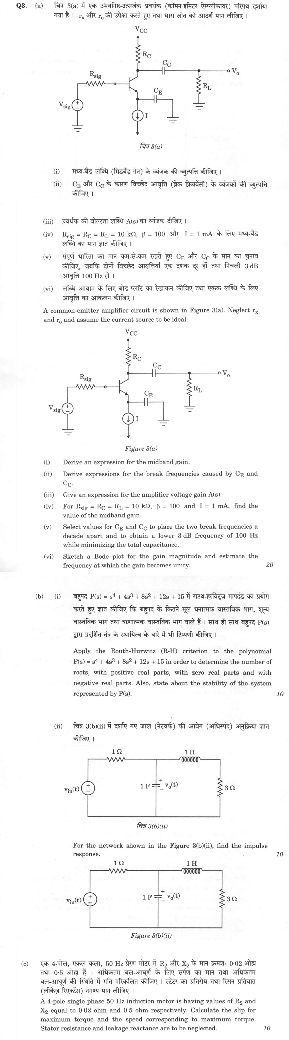
A common-emitter amplifier circuit is shown in Figure 3(a). Neglect r_x and r_o and assume the current source to be ideal. (i)…
A common-emitter amplifier circuit is shown in Figure 3(a). Neglect r_x and r_o and assume the current source to be ideal.
Derive an expression for the midband gain.
Derive expressions for the break frequencies caused by C_E and C_C.
Give an expression for the amplifier voltage gain A(s).
For R_sig = R_C = R_L = 10 kΩ, β = 100 and I = 1 mA, find the value of the midband gain.
Select values for C_E and C_C to place the two break frequencies a decade apart and to obtain a lower 3 dB frequency of 100 Hz while minimizing the total capacitance.
Sketch a Bode plot for the gain magnitude and estimate the frequency at which the gain becomes unity.
Apply the Routh-Hurwitz (R-H) criterion to the polynomial P(s) = s⁴ + 4s³ + 8s² + 12s + 15 in order to determine the number of roots, with positive real parts, with zero real parts and with negative real parts. Also, state about the stability of the system represented by P(s).
For the network shown in the Figure 3(b)(ii), find the impulse response.
A 4-pole single phase 50 Hz induction motor is having values of R₂ and X₂ equal to 0·02 ohm and 0·5 ohm respectively. Calculate the slip for maximum torque and the speed corresponding to maximum torque. Stator resistance and leakage reactance are to be neglected.
हिंदी में प्रश्न पढ़ें
चित्र 3(a) में एक उभयनिष्ठ-उत्सर्जक प्रवर्धक (कॉमन-एमिटर एम्पलीफायर) परिपथ दर्शाया गया है । rₓ और r₀ की उपेक्षा करते हुए तथा धारा स्रोत को आदर्श मान लीजिए ।
मध्य-बैंड लाभिधि (मिडबैंड गेन) के व्यंजक की व्युत्पत्ति कीजिए ।
Cᴇ और Cᴄ के कारण विच्छेद आवृत्ति (ब्रेक फ्रीक्वेंसी) के व्यंजकों की व्युत्पत्ति कीजिए ।
प्रवर्धक की वोल्टता लाभिधि A(s) का व्यंजक दीजिए ।
R_sig = R_C = R_L = 10 kΩ, β = 100 और I = 1 mA के लिए मध्य-बैंड लाभिधि का मान ज्ञात कीजिए ।
संपूर्ण धारिता का मान कम-से-कम रखते हुए C_E और C_C के मान का चुनाव कीजिए, जबकि दोनों विच्छेद आवृत्तियाँ एक दशक दूर हों तथा निचली 3 dB आवृत्ति 100 Hz हो ।
लाभिधि आयाम के लिए बोड प्लॉट का रेखांकन कीजिए तथा एकक लाभिधि के लिए आवृत्ति का आकलन कीजिए ।
बहुपद P(s) = s⁴ + 4s³ + 8s² + 12s + 15 में राउथ-हरविट्ज मापदंड का प्रयोग करते हुए ज्ञात कीजिए कि बहुपद के कितने मूल धनात्मक वास्तविक भाग, शून्य वास्तविक भाग तथा ऋणात्मक वास्तविक भाग वाले हैं। साथ ही साथ बहुपद P(s) द्वारा प्रदर्शित तंत्र के स्थायित्व के बारे में भी टिप्पणी कीजिए ।
चित्र 3(b)(ii) में दर्शाए गए जाल (नेटवर्क) की आवेग (अधिस्पंद) अनुक्रिया ज्ञात कीजिए ।
एक 4-पोल, एकल कला, 50 Hz प्रेरण मोटर में R₂ और X₂ के मान क्रमशः 0·02 ओह तथा 0·5 ओह है । अधिकतम बल-आघूर्ण के लिए सर्पण का मान तथा अधिकतम बल-आघूर्ण की स्थिति में गति परिकलित कीजिए । स्टेटर का प्रतिरोध तथा रिसन प्रतिघात (लीकेज रिएक्टेंस) नगण्य मान लीजिए ।
The figure this question refers to, in words
The question paper is a scan and the diagram did not survive as text. This is the figure as read from the original page — every component, value and label — so the question can be worked from the text below.
(a) A common-emitter amplifier circuit diagram. The input signal source V_sig is connected in series with a resistor R_sig to the base of an NPN transistor. The emitter of the transistor is connected to ground through a current source labeled I (pointing downwards) and in parallel with a capacitor C_E. The collector of the transistor is connected to the positive supply rail V_CC through a resistor R_C. The collector node is also connected to the output terminal V_o through a coupling capacitor C_C. The output terminal V_o is connected to ground through a load resistor R_L. The circuit is labeled 'Figure 3(a)'.
(b) Figure 3(b)(ii) shows an electrical circuit. On the left, a voltage source labeled v_in(t) is connected in series with a 1 Ohm resistor. The resistor connects to a central node. From this node, a 1 Farad capacitor is connected to the bottom reference line (ground). The voltage across this capacitor is labeled v_o(t) with the positive terminal at the top. Also connected to this central node is a 1 Henry inductor in series with a 3 Ohm resistor, which then connects to the bottom reference line. The bottom of the voltage source, the bottom of the capacitor, and the bottom of the 3 Ohm resistor are all connected together.
(c) A single-phase full-bridge inverter circuit diagram labeled 'Figure 2(c)'. The input source is labeled '200 V, 50 Hz' connected to the top and bottom rails of the bridge. The bridge consists of four thyristors arranged in two legs. The left leg contains thyristor T1 (top) and T4 (bottom). The right leg contains thyristor T3 (top) and T2 (bottom). The thyristors are connected in series within each leg, with the midpoint of the left leg connected to the midpoint of the right leg. The load is a resistor labeled 'R' connected across the output terminals of the bridge (the top of the right leg and the bottom of the right leg). The current flowing into the load resistor is labeled 'iL' with an arrow pointing to the right.
A common-emitter amplifier circuit diagram. A DC voltage source V_CC is connected to the top of a resistor R_C. The bottom of R_C connects to the collector of an NPN transistor. The base of the transistor is connected to a signal source V_sig in series with a resistor R_sig. The emitter of the transistor is connected to a capacitor C_E which goes to ground, and also to an ideal current source I which goes to ground. The collector node is also connected to a coupling capacitor C_C, which connects to a load resistor R_L. The other end of R_L is grounded. The output voltage V_o is taken across R_L. The text specifies to neglect r_x and r_o.
What "Derive" is asking you to do
Reach the stated expression from a starting relation, justifying every step. The destination is printed in the question, so only the route earns marks, and the assumptions you work under are part of that route.
Structure that answers it
Assumptions and notation defined → starting relation or governing equation → each step with its justification → the required expression → limiting case or boundary check
Where marks are lost
Writing the standard result first and fitting three lines to it, which an examiner reads at a glance. Marks also go on assumptions left unstated — lossless medium, small amplitude, errors independent with zero mean — and on symbols used before they are defined, even when the question says usual notations.
How this answer will be evaluated
Approach
(a(i)) derive: given > assumptions > stepwise derivation > result > check | (a(ii)) derive: given > assumptions > stepwise derivation > result > check | (a(iii)) derive: given > assumptions > stepwise derivation > result > check | (a(iv)) calculate: given > formula > substitution > result with units > interpretation | (a(v)) calculate: given > formula > substitution > result with units > interpretation | (a(vi)) describe: define > structure or process in order > labelled diagram > significance | (b(i)) analyse: intro > causes > effects > stakeholders/linkages > way forward | (b(ii)) calculate: given > formula > substitution > result with units > interpretation | (c) calculate: given > formula > substitution > result with units > interpretation Full marks: Complete derivations with correct equivalent circuits, accurate calculations, and clear physical interpretation.
Key points expected
- Small-signal equivalent circuit drawn
- Transconductance gm expressed in terms of I
- Input resistance rπ identified
- Gain formula derived stepwise
- Low-frequency equivalent circuit for CE
- Low-frequency equivalent circuit for CC
- Time constants identified for each
- Break frequency formulas derived
Evaluation rubric
Each sub-part is marked on its own, against the marks and word limit printed on the paper.
- (a(i)) Expression for midband voltage gain of the common-emitter amplifier.
derive— given → assumptions → stepwise derivation → result → check
Must cover
- Small-signal equivalent circuit drawn
- Transconductance gm expressed in terms of I
- Input resistance rπ identified
- Gain formula derived stepwise
Loses marks
- Formula stated without derivation
- Sign error in gain expression
Earns more
- Explicit assumption of ideal current source
- Neglect of ro and rx stated
Extra mark
- Phasor diagram included
- (a(ii)) Expressions for break frequencies caused by CE and CC.
derive— given → assumptions → stepwise derivation → result → check
Must cover
- Low-frequency equivalent circuit for CE
- Low-frequency equivalent circuit for CC
- Time constants identified for each
- Break frequency formulas derived
Loses marks
- Missing equivalent circuit for either capacitor
- Incorrect resistance calculation
Earns more
- Resistance seen by each capacitor calculated
- Assumptions for midband vs low-freq stated
Extra mark
- Bode plot sketch for individual poles
- (a(iii)) Expression for amplifier voltage gain A(s).
derive— given → assumptions → stepwise derivation → result → check
Must cover
- Transfer function in s-domain
- Poles from CE and CC included
- Midband gain as DC limit
- Algebraic steps shown
Loses marks
- Missing s-dependence in gain
- Algebraic errors in transfer function
Earns more
- Zeros identified if present
- Dimensional consistency checked
Extra mark
- Block diagram representation
- (a(iv)) Numerical value of midband gain for given parameters.
calculate— given → formula → substitution → result with units → interpretation
Must cover
- gm calculated from I = 1 mA
- rπ calculated from β and gm
- Gain formula substituted with values
- Final gain with units
Loses marks
- Arithmetic error in substitution
- Missing units in final answer
Earns more
- Intermediate values shown
- Units carried through calculation
Extra mark
- Comparison with theoretical max gain
- (a(v)) Values of CE and CC for specified frequency response.
calculate— given → formula → substitution → result with units → interpretation
Must cover
- Break frequencies set 1 decade apart
- Lower 3dB frequency = 100 Hz
- Capacitance values calculated
- Total capacitance minimized
Loses marks
- Incorrect frequency assignment
- Missing minimization step
Earns more
- Optimization constraint shown
- Verification of frequency separation
Extra mark
- Sensitivity analysis of capacitance
- (a(vi)) Bode plot sketch and unity gain frequency estimate.
describe— define → structure or process in order → labelled diagram → significance
Must cover
- Magnitude plot with correct slopes
- Break frequencies marked
- Unity gain frequency estimated
- Phase plot if included
Loses marks
- Incorrect slope at break frequencies
- Missing unity gain frequency
Earns more
- Asymptotic approximation shown
- Gain margin indicated
Extra mark
- Stability comment from Bode plot
- (b(i)) Routh-Hurwitz analysis of polynomial P(s).
analyse— intro → causes → effects → stakeholders/linkages → way forward
Must cover
- Routh array constructed correctly
- Sign changes counted
- Roots classified by real part
- Stability conclusion stated
Loses marks
- Error in Routh array construction
- Incorrect stability conclusion
Earns more
- Auxiliary polynomial if needed
- Explicit count of each root type
Extra mark
- Root locus sketch
- (b(ii)) Impulse response of the given network.
calculate— given → formula → substitution → result with units → interpretation
Must cover
- Circuit converted to s-domain
- Transfer function H(s) derived
- Inverse Laplace transform performed
- Time-domain response expressed
Loses marks
- Missing s-domain conversion
- Incorrect inverse Laplace transform
Earns more
- Pole-zero plot of H(s)
- Initial and final value checks
Extra mark
- Step response comparison
- (c) Slip and speed for maximum torque in induction motor.
calculate— given → formula → substitution → result with units → interpretation
Must cover
- Synchronous speed calculated
- Slip for max torque formula used
- Numerical slip value computed
- Rotor speed calculated
Loses marks
- Incorrect synchronous speed calculation
- Missing slip formula derivation
Earns more
- Assumptions stated (neglect stator impedance)
- Units for all quantities
Extra mark
- Torque-slip curve sketch
Model answer coming soon
Every evaluation on this site is marked against a verified model answer. This question's answer is still being written; evaluation opens the moment it lands.
More from Electrical Engineering 2022 Paper I
- Q1 (a) For the circuit shown in Figure 1(a), find the V_in, V_S and power supplied by the de…
- Q2 (a) (i) For the circuit shown in Figure 2(a)(i), initial current through the coil is zero…
- Q3 A common-emitter amplifier circuit is shown in Figure 3(a). Neglect r_x and r_o and assum…
- Q4 For the network shown in Figure 4(a)(i) and its excitation function shown in Figure 4(a)(…
- Q5 (a) The diagram of Master-Slave S-R flip-flop and the waveform applied to the Master flip…
- Q6 (a) The plane wave E = 30 cos (ωt – z) aₓ V/m in air normally hits a lossless medium (μ =…