Paper I — Q3
(a) Determine the time signal that corresponds to the following bilateral Laplace transform and the ROCs given below by using the…
Determine the time signal that corresponds to the following bilateral Laplace transform and the ROCs given below by using the method of partial fractions:
X(s) = (4s² + 8s + 10)/((s+2)(s² + 2s + 5))
With ROC Re(s) < -2
With ROC Re(s) > -1
With ROC -2 < Re(s) < -1
Explain the working of the given OPAMP circuit. Draw the output waveforms at points A and B showing the time and voltage.
Given that, V_Z₁ = V_Z₂ = 3.3 V, C₁ = 1 muF, the power supply voltage to OPAMPs is ± 12 V and R₁ = R₂ = R₃ = R₄ = R₅ = R₆ = 2 kΩ :
Suggest to replace suitable resistances so that the output voltages at A and B are having swing of ± 6 V and the output frequency is fixed to 500 Hz.
Find the logic equations for the outputs in the concise form and write the corresponding truth table for the circuit given below :
हिंदी में प्रश्न पढ़ें
नीचे दिए गए द्विपक्षीय लाप्लास रूपांतर और ROCs के अनुरूप समय संकेत, आंशिक भिन्न विधि प्रयोग करते हुए ज्ञात कीजिए :
X(s) = (4s² + 8s + 10)/((s+2)(s² + 2s + 5))
ROC Re(s) < -2 के साथ
ROC Re(s) > -1 के साथ
ROC -2 < Re(s) < -1 के साथ
दिए गए OPAMP परिपथ की कार्यप्रणाली की व्याख्या कीजिए। समय व बोल्टता प्रदर्शित करते हुए बिंदु A तथा B पर निर्गत तरंग रूप आरेखित कीजिए।
दिया गया है, V_Z₁ = V_Z₂ = 3.3 V, C₁ = 1 muF, OPAMP को प्रदत्त शक्ति प्रदाय बोल्टता ± 12 V है तथा R₁ = R₂ = R₃ = R₄ = R₅ = R₆ = 2 kΩ है :
उपयुक्त प्रतिरोधों में बदलाव प्रस्तावित कीजिए ताकि A और B पर निर्गत बोल्टता परास ± 6 V हो जाए तथा निर्गत आवृत्ति 500 Hz हो जाए।
नीचे दिए गए परिपथ के आउटपुट के लिए संक्षिप्त तार्किक समीकरण निकालिए और तदनुरूप सत्य-सारणी लिखिए :
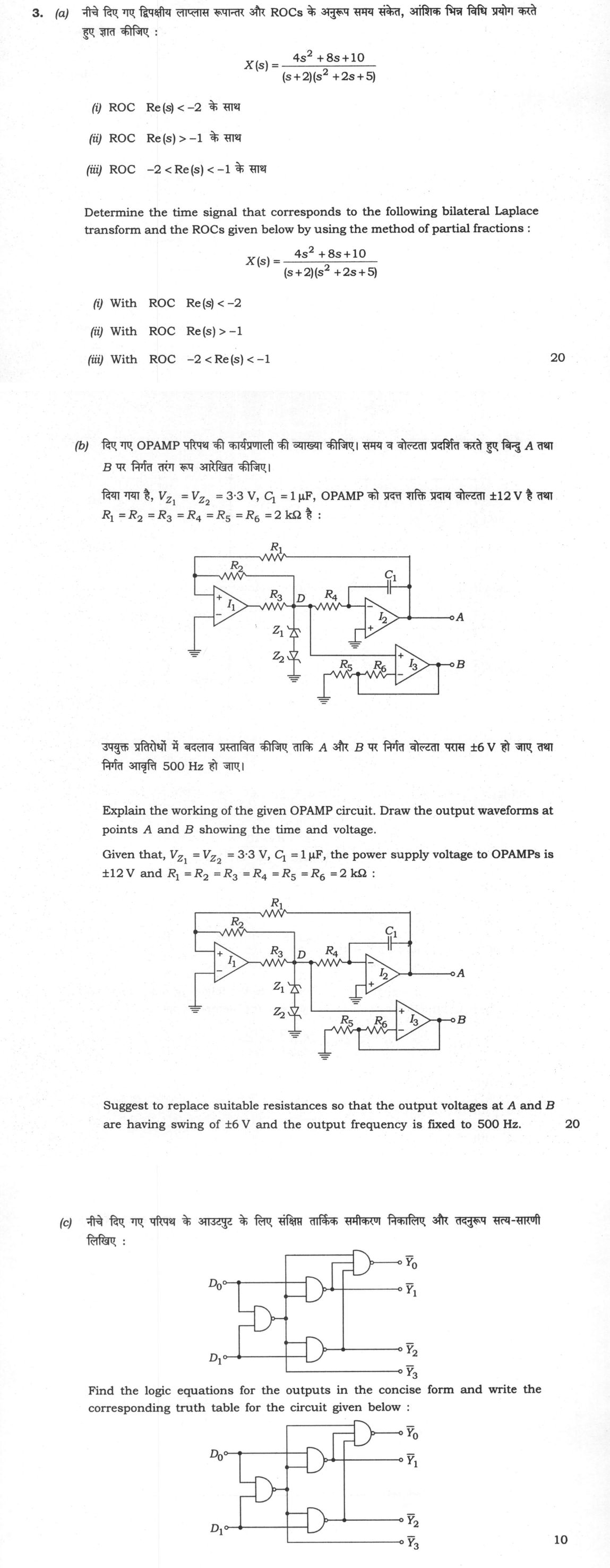
The figure this question refers to, in words
The question paper is a scan and the diagram did not survive as text. This is the figure as read from the original page — every component, value and label — so the question can be worked from the text below.
(b) An electronic circuit diagram consisting of three operational amplifiers (OPAMPs) labeled I1, I2, and I3, and two Zener diodes labeled Z1 and Z2. The circuit is powered by a supply voltage (implied +/-12V).
- OPAMP I1 is configured as a comparator. Its non-inverting input (+) is connected to a node formed by resistors R1 and R2. R1 is connected to the output of OPAMP I2 (labeled point A). R2 is connected to the output of OPAMP I3 (labeled point B). The inverting input (-) of I1 is connected to ground. The output of I1 is connected to a node labeled D via resistor R3.
- Node D is connected to the anode of Zener diode Z1 (cathode to ground) and the cathode of Zener diode Z2 (anode to ground). This node D is also connected to the inverting input (-) of OPAMP I2 via resistor R4.
- OPAMP I2 is configured as an integrator. Its non-inverting input (+) is connected to ground. Its inverting input (-) is connected to node D via R4 and to its own output (point A) via capacitor C1. The output is labeled A.
- The output of OPAMP I2 (point A) is also connected to the non-inverting input (+) of OPAMP I3.
- OPAMP I3 is configured as a comparator. Its inverting input (-) is connected to a voltage divider formed by resistors R5 and R6. R5 is connected to ground, and R6 is connected to the output of I3 (point B). The junction of R5 and R6 connects to the inverting input. The output is labeled B.
All components are labeled with their reference designators (R1-R6, C1, Z1, Z2, I1-I3) and nodes (A, B, D).
(c) A logic circuit diagram with two inputs, D0 and D1, and four outputs, Y0, Y1, Y2, and Y3 (all with overbars indicating active-low or inverted outputs). The circuit consists of four 2-input NAND gates. The inputs D0 and D1 are connected to the gates as follows: 1. The top gate (output Y0) has inputs D0 and D1. 2. The second gate (output Y1) has inputs D0 and the output of the third gate. 3. The third gate (output Y2) has inputs D1 and the output of the fourth gate. 4. The bottom gate (output Y3) has inputs D0 and D1. The outputs of the third and fourth gates are also fed back into the second and third gates respectively, creating a cross-coupled structure. The specific connections are: D0 and D1 go to the top gate. D0 and the output of the bottom gate go to the second gate. D1 and the output of the third gate go to the third gate. D0 and D1 go to the bottom gate. The outputs are labeled Y0, Y1, Y2, Y3 from top to bottom.
What "Solve" is asking you to do
Choose the method, then carry it through to a final answer. Identifying what kind of problem this is and why that method applies is the first thing marked; a correct figure arrived at invisibly earns almost nothing.
Structure that answers it
Given data and what is required → method chosen, with the reason it applies → set-up (equation, circuit, free body, trial balance) → working, step by step → answer with units and any condition of validity
Where marks are lost
Doing the middle steps mentally and writing only the result. In mathematics papers, a further loss comes from giving a decimal where the exact value in surds or fractions was wanted, or from skipping the justification a part explicitly asks for.
How this answer will be evaluated
Approach
Framework: Bilateral Laplace Transform Inversion & Op-Amp Oscillator Analysis. (a) calculate: given > formula > substitution > result with units > interpretation | (b) explain: definition/context > points in order > small example > short close | (c) calculate: given > formula > substitution > result with units > interpretation Full marks: Accurate partial fractions, correct ROC application, clear circuit analysis, precise logic derivation.
Key points expected
- Partial fraction expansion
- ROC-based signal determination
- Astable multivibrator operation
- Zener diode clamping
- Frequency and amplitude calculation
- Boolean logic simplification
- Truth table construction
Evaluation rubric
Each sub-part is marked on its own, against the marks and word limit printed on the paper.
- (a) Inverse Laplace transform for three specific ROCs using partial fractions.
calculate— given → formula → substitution → result with units → interpretation
Must cover
- Partial fraction expansion of X(s)
- Identification of poles at s=-2, -1±j2
- Correct time-domain signal for each ROC
- Application of causality/anti-causality based on ROC
Loses marks
- Ignoring ROC constraints on signal type
- Algebraic errors in partial fractions
Earns more
- Explicit calculation of residues
- Clear labeling of (i), (ii), (iii) results
- Correct use of u(t) and u(-t) terms
Extra mark
- Sketch of pole-zero plot with ROCs
- (b) Working of Op-Amp circuit, waveforms at A and B, and component values for 500Hz/±6V. 20 marks
explain— definition/context → points in order → small example → short close
Must cover
- Identification of circuit as Astable Multivibrator
- Explanation of Zener diode clamping action
- Derivation of frequency and amplitude formulas
- Calculation of new R and C values for 500Hz
Loses marks
- Confusing inverting/non-inverting inputs
- Incorrect frequency formula application
Earns more
- Sketch of waveforms at A and B
- Step-by-step calculation of R1, R2, C1
- Explanation of hysteresis loop
Extra mark
- Circuit diagram with labeled nodes
- (c) Logic equations for outputs and corresponding truth table. 10 marks
calculate— given → formula → substitution → result with units → interpretation
Must cover
- Boolean expression for each output Y0-Y3
- Simplification of logic equations
- Complete truth table for inputs D0, D1
- Correct mapping of inputs to outputs
Loses marks
- Incorrect gate identification
- Missing rows in truth table
Earns more
- Use of K-map for simplification
- Clear labeling of logic gates
- Verification of equations with truth table
Extra mark
- Circuit diagram with labeled gates
Model answer coming soon
Every evaluation on this site is marked against a verified model answer. This question's answer is still being written; evaluation opens the moment it lands.
More from Electrical Engineering 2024 Paper I
- Q1 (a) Find the voltage on points A and B of the given circuit : (10 marks) (b) Determine th…
- Q2 (a) Draw the circuit diagram, function table, logic symbol and switch model for a CMOS ga…
- Q3 (a) Determine the time signal that corresponds to the following bilateral Laplace transfo…
- Q4 (a) In the circuit diagram given here, load resistance R_L is to be set for maximum power…
- Q5 (a) A uniform plane wave travels in vacuum along +y direction. The electric field of the…
- Q6 (a) (i) An AM signal s(t) = A_c[1 + kₐ m(t)]cos(2πf_c t) is applied to the system shown i…