Paper II — Q7
(a) Calculate the real and reactive power at sending end of a transmission line while delivering 10 MVA load at 0·85 lagging…
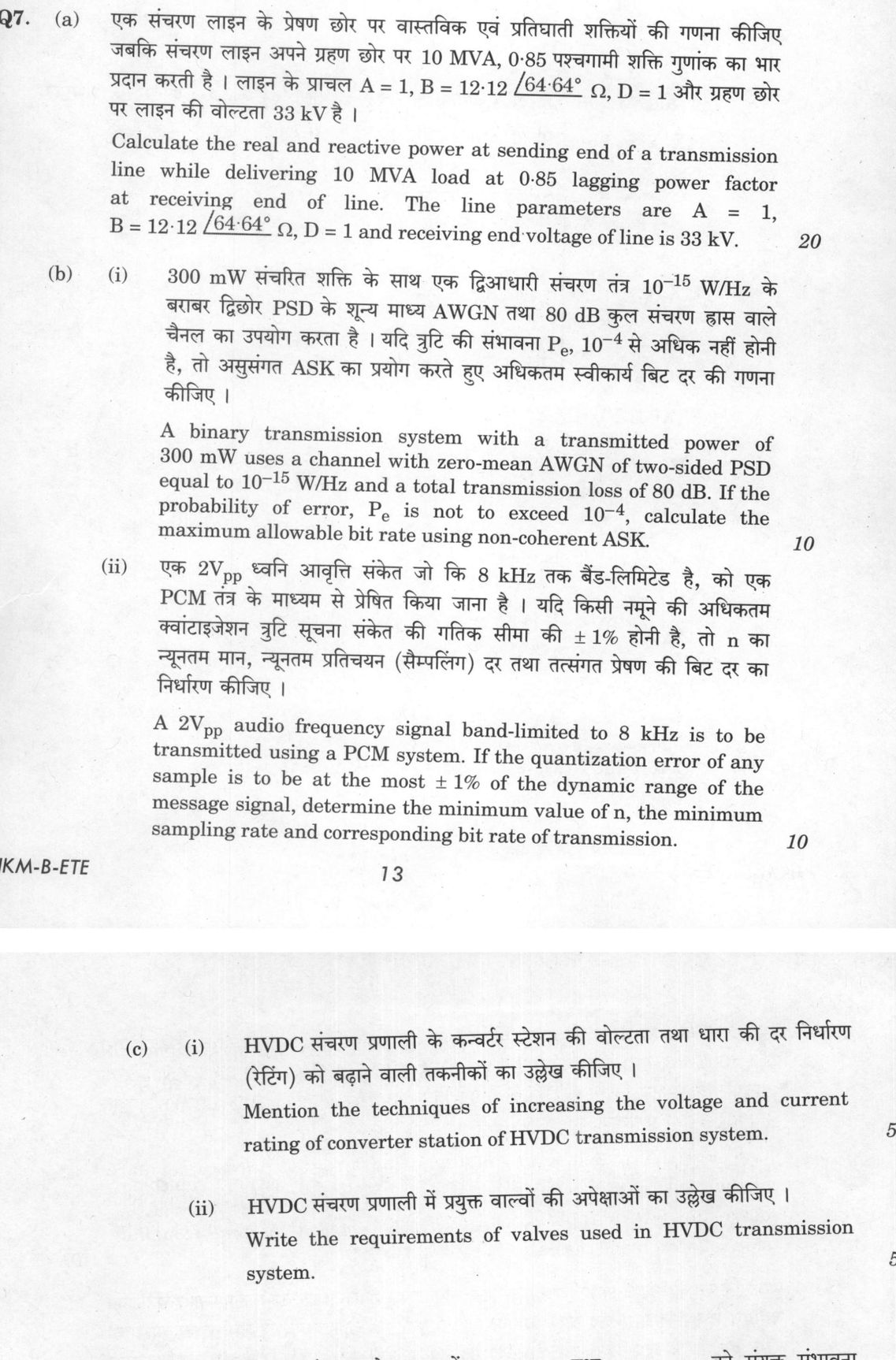
Calculate the real and reactive power at sending end of a transmission line while delivering 10 MVA load at 0·85 lagging power factor at receiving end of line. The line parameters are A = 1, B = 12·12 ∠64·64° Ω, D = 1 and receiving end voltage of line is 33 kV. 20 marks
A binary transmission system with a transmitted power of 300 mW uses a channel with zero-mean AWGN of two-sided PSD equal to 10⁻¹⁵ W/Hz and a total transmission loss of 80 dB. If the probability of error, Pₑ is not to exceed 10⁻⁴, calculate the maximum allowable bit rate using non-coherent ASK. 10 marks
A 2Vₚₚ audio frequency signal band-limited to 8 kHz is to be transmitted using a PCM system. If the quantization error of any sample is to be at the most ±1% of the dynamic range of the message signal, determine the minimum value of n, the minimum sampling rate and corresponding bit rate of transmission. 10 marks
Mention the techniques of increasing the voltage and current rating of converter station of HVDC transmission system. 5 marks
Write the requirements of valves used in HVDC transmission system. 5 marks
हिंदी में प्रश्न पढ़ें
एक संचरण लाइन के प्रेषण छोर पर वास्तविक एवं प्रतिघाती शक्तियों की गणना कीजिए जबकि संचरण लाइन अपने ग्रहण छोर पर 10 MVA, 0·85 पश्चगामी शक्ति गुणांक का भार प्रदान करती है । लाइन के प्राचल A = 1, B = 12·12 ∠64·64° Ω, D = 1 और ग्रहण छोर पर लाइन की वोल्टता 33 kV है । (20 अंक)
300 mW संचरित शक्ति के साथ एक द्विआधारी संचरण तंत्र 10⁻¹⁵ W/Hz के बराबर द्विशोर PSD के शून्य माध्य AWGN तथा 80 dB कुल संचरण ह्रास वाले चैनल का उपयोग करता है । यदि त्रुटि की संभावना Pₑ, 10⁻⁴ से अधिक नहीं होनी है, तो असुसंगत ASK का प्रयोग करते हुए अधिकतम स्वीकार्य बिट दर की गणना कीजिए । (10 अंक)
एक 2Vₚₚ ध्वनि आवृत्ति संकेत जो कि 8 kHz तक बैंड-लिमिटेड है, को एक PCM तंत्र के माध्यम से प्रेषित किया जाना है । यदि किसी नमूने की अधिकतम क्वांटाइजेशन त्रुटि सूचना संकेत की गतिक सीमा की ±1% होनी है, तो n का न्यूनतम मान, न्यूनतम प्रतिचयन (सैंपलिंग) दर तथा तत्संगत प्रेषण की बिट दर का निर्धारण कीजिए । (10 अंक)
HVDC संचरण प्रणाली के कनवर्टर स्टेशन की वोल्टता तथा धारा की दर निर्धारण (रेटिंग) को बढ़ाने वाली तकनीकों का उल्लेख कीजिए । (5 अंक)
HVDC संचरण प्रणाली में प्रयुक्त वाल्वों की अपेक्षाओं का उल्लेख कीजिए । (5 अंक)
Model answer
Written by UPSC Answer Check against this question's marking rubric, to the expected length. UPSC does not publish answers for Mains — this is one way to score well, not an official key.
(a) For a reciprocal passive two-port line, AD − BC = 1. Given A = 1 and D = 1, 1 − B C = 1, so C = 0. Hence the line behaves as a series element B, and Is = Ir.
Receiving-end load: Sᵣ = 10 MVA, pf = 0.85 lagging. Pᵣ = 10 × 0.85 = 8.5 MW. Qᵣ = 10 × sin(cos⁻¹0.85) = 10 × 0.5268 = 5.2678 MVAr lagging.
Receiving-end line voltage = 33 kV. Iᵣ = Sᵣ/(√3 V_LL) = 10 × 10⁶/(√3 × 33 × 10³) = 174.955 A.
Taking Vᵣ as reference, for lagging load: Iᵣ = 174.955∠−31.79° A.
B = 12.12∠64.64° Ω, so R = 12.12 cos64.64° = 5.191 Ω, X = 12.12 sin64.64° = 10.952 Ω. |Iᵣ|² = (174.955)² = 3.0609 × 10⁴ A².
Since Is = Iᵣ, sending-end three-phase complex power is Ss = 3Vs Is* = 3Vᵣ Iᵣ* + 3B|Iᵣ|² = Sᵣ + 3(R + jX)|Iᵣ|².
Active line loss: 3R|Iᵣ|² = 3 × 5.191 × 3.0609 × 10⁴ = 4.766 × 10⁵ W = 0.4767 MW.
Reactive absorption: 3X|Iᵣ|² = 3 × 10.952 × 3.0609 × 10⁴ = 1.0057 × 10⁶ VAr = 1.0057 MVAr.
Therefore, Pₛ = 8.5 + 0.4767 = 8.9767 MW. Qₛ = 5.2678 + 1.0057 = 6.2735 MVAr lagging.
Pₛ = 8.977 MW, Qₛ = 6.274 MVAr (lagging).
(b)(i) For ideal non-coherent ASK envelope detection, Pₑ = ½ exp[−E_b/(2N₀)].
Transmitted power = 300 mW = 0.3 W. Total loss = 80 dB, so received power is Pᵣ = 0.3/10⁸ = 3 × 10⁻⁹ W.
Given two-sided noise PSD = 10⁻¹⁵ W/Hz, the one-sided PSD is N₀ = 2 × 10⁻¹⁵ W/Hz.
Set Pₑ ≤ 10⁻⁴: ½ exp[−E_b/(2N₀)] ≤ 10⁻⁴ exp[−E_b/(2N₀)] ≤ 2 × 10⁻⁴ E_b/(2N₀) ≥ −ln(2 × 10⁻⁴) = 8.517 E_b ≥ 17.034 N₀ = 17.034 × 2 × 10⁻¹⁵ = 3.4068 × 10⁻¹⁴ J.
Maximum bit rate: R_b,max = Pᵣ/E_b,min = 3 × 10⁻⁹/(3.4068 × 10⁻¹⁴) = 8.806 × 10⁴ bit/s.
R_b,max ≈ 8.81 × 10⁴ bit/s = 88.1 kbit/s.
(b)(ii) Signal: 2 V peak-to-peak, so dynamic range = 2 V. Maximum quantization error = Δ/2. Condition: Δ/2 ≤ 1% of 2 V = 0.02 V. Thus Δ ≤ 0.04 V.
Number of levels L ≥ 2/0.04 = 50. n = ⌈log₂50⌉ = 6, since 2⁵ = 32 < 50 ≤ 64 = 2⁶.
Check: with n = 6, Δ = 2/64 = 0.03125 V, maximum error = Δ/2 = 0.015625 V = 0.781% < 1%.
Band-limited to 8 kHz, so minimum sampling rate: fs,min = 2 × 8 kHz = 16 kHz = 16,000 samples/s.
Bit rate: R_b = n fs = 6 × 16,000 = 96,000 bit/s.
n = 6 bits; fs,min = 16 kHz; R_b = 96 kbit/s.
(c)(i) Techniques for increasing voltage rating:
- Series connection of thyristors/IGBTs in each valve, with grading resistors and RC snubbers for steady-state and dynamic voltage sharing.
- Series connection of converter bridges or MMC submodules per pole; use of 12-pulse/24-pulse configurations.
- Improved insulation coordination, higher insulation levels, oil/SF₆/air insulation and suitable bushings.
Techniques for increasing current rating:
- Parallel connection of thyristors/IGBT modules or valves, with current-sharing reactors and symmetrical busbar layout.
- Parallel converter bridges/poles and interphase reactors.
- Efficient water cooling, high-current semiconductor wafers, and redundancy for reliability.
(c)(ii) Requirements of HVDC valves:
- High repetitive peak forward and reverse voltage capability, transient overvoltage and dv/dt withstand.
- Rated continuous current, overload and surge/fault current capability, high di/dt withstand.
- Low conduction and switching losses, reliable gate firing and fast protection.
- Uniform voltage sharing in series strings and current sharing in parallel strings.
- Adequate insulation, creepage/clearance, cooling, mechanical/seismic strength.
- High reliability, availability, easy maintenance and monitoring.
What "Calculate" is asking you to do
Apply the standard formula or schedule to data the question has already supplied — a table of readings, cost records, a balance sheet — and produce the number. The method is rarely in doubt; the marks sit in the named intermediate quantities, each of which has to appear as a labelled line.
Structure that answers it
Data as given → formula or standard treatment, named → substitution → each intermediate, labelled → result with units
Where marks are lost
Omitting an intermediate the marking scheme pays for separately, or rounding at an intermediate line so the final figure drifts. In commerce and accountancy, any figure in a statement that no numbered working note supports is treated as unearned.
How this answer will be evaluated
Approach
(a) calculate: given > formula > substitution > result with units > interpretation | (b(i)) calculate: given > formula > substitution > result with units > interpretation | (b(ii)) calculate: given > formula > substitution > result with units > interpretation | (c(i)) describe: define > structure or process in order > labelled diagram > significance | (c(ii)) describe: define > structure or process in order > labelled diagram > significance Full marks: Complete working with correct phasor diagrams, accurate calculations, and clear explanations of HVDC concepts.
Key points expected
- State receiving end complex power S_R from 10 MVA and 0.85 pf
- Calculate receiving end current I_R using V_R and S_R
- Apply sending end voltage equation V_S = AV_R + BI_R
- Compute sending end complex power S_S = V_S I_S*
- Calculate received power P_R from 300 mW and 80 dB loss
- State non-coherent ASK P_e formula involving Q function
- Determine required SNR or energy per bit E_b for P_e = 10^-4
- Relate E_b to bit rate R_b using P_R = E_b R_b
Evaluation rubric
Each sub-part is marked on its own, against the marks and word limit printed on the paper.
- (a) Determine sending end real and reactive power using ABCD parameters. 20 marks
calculate— given → formula → substitution → result with units → interpretation
Must cover
- State receiving end complex power S_R from 10 MVA and 0.85 pf
- Calculate receiving end current I_R using V_R and S_R
- Apply sending end voltage equation V_S = AV_R + BI_R
- Compute sending end complex power S_S = V_S I_S*
Loses marks
- Using real power P instead of complex power S for current
- Ignoring the phase angle of B parameter in calculation
- Sign errors in phasor addition for V_S
Earns more
- Explicit calculation of I_S using D and C parameters
- Phasor diagram showing V_R, I_R, and V_S relationship
- Verification of power balance or line losses
Extra mark
- Calculation of line losses to verify S_S - S_R
- (b(i)) Find maximum bit rate for non-coherent ASK given P_e and noise PSD. 10 marks
calculate— given → formula → substitution → result with units → interpretation
Must cover
- Calculate received power P_R from 300 mW and 80 dB loss
- State non-coherent ASK P_e formula involving Q function
- Determine required SNR or energy per bit E_b for P_e = 10^-4
- Relate E_b to bit rate R_b using P_R = E_b R_b
Loses marks
- Confusing one-sided and two-sided PSD in noise power
- Using coherent ASK formula instead of non-coherent
- Incorrect dB to linear conversion for transmission loss
Earns more
- Explicit calculation of noise power N_0/2
- Correct use of Q^-1(10^-4) value
Extra mark
- Comparison with coherent ASK performance
- (b(ii)) Determine PCM parameters n, sampling rate, and bit rate. 10 marks
calculate— given → formula → substitution → result with units → interpretation
Must cover
- Calculate minimum n from quantization error ±1% of dynamic range
- Apply Nyquist theorem for minimum sampling rate from 8 kHz
- Calculate bit rate as product of n and sampling rate
- State dynamic range from 2V_pp signal
Loses marks
- Using 0.5% instead of 1% for quantization error
- Forgetting to double frequency for Nyquist rate
- Confusing peak-to-peak voltage with peak voltage
Earns more
- Explicit formula for quantization step size ΔV
- Clear statement of Nyquist criterion f_s ≥ 2f_m
Extra mark
- Mention of oversampling factor if applicable
- (c(i)) List techniques for increasing HVDC converter station ratings. 5 marks
describe— define → structure or process in order → labelled diagram → significance
Must cover
- Mention series connection of valves for voltage increase
- Mention parallel connection of valves for current increase
- Reference to multi-level converter topologies
- Mention of series-parallel combinations
Loses marks
- Confusing AC and DC rating increase techniques
- Vague statements without specific valve configurations
Earns more
- Brief explanation of how each technique works
- Mention of specific converter types like LCC or VSC
Extra mark
- Mention of specific HVDC project examples
- (c(ii)) State requirements for HVDC transmission system valves. 5 marks
describe— define → structure or process in order → labelled diagram → significance
Must cover
- High voltage blocking capability in both directions
- Fast switching speed for control and protection
- High current carrying capacity
- Reliability and long operational life
Loses marks
- Listing generic power electronics requirements without HVDC context
- Omitting bidirectional blocking capability
Earns more
- Mention of thermal management requirements
- Reference to specific valve types like thyristors or IGBTs
Extra mark
- Mention of specific voltage/current ratings for modern HVDC
Practice this exact question
Write your answer and it is marked point by point against the model answer above — what you covered, what you missed, what you got wrong.
Evaluate my answer →More from Electrical Engineering 2024 Paper II
- Q4 (a) The capacitance of a piezoelectric transducer is 2000 pF and charge sensitivity is 30…
- Q5 (a) The block diagram of a position control system is shown in the figure. Determine the…
- Q6 (a) Calculate the power loss in the transmission system given in the following figure. Th…
- Q7 (a) Calculate the real and reactive power at sending end of a transmission line while del…
- Q8 (a) Two sources M₁ and M₂ emit messages x₁, x₂, x₃ and y₁, y₂, y₃ with the joint probabil…