Paper I — Q3
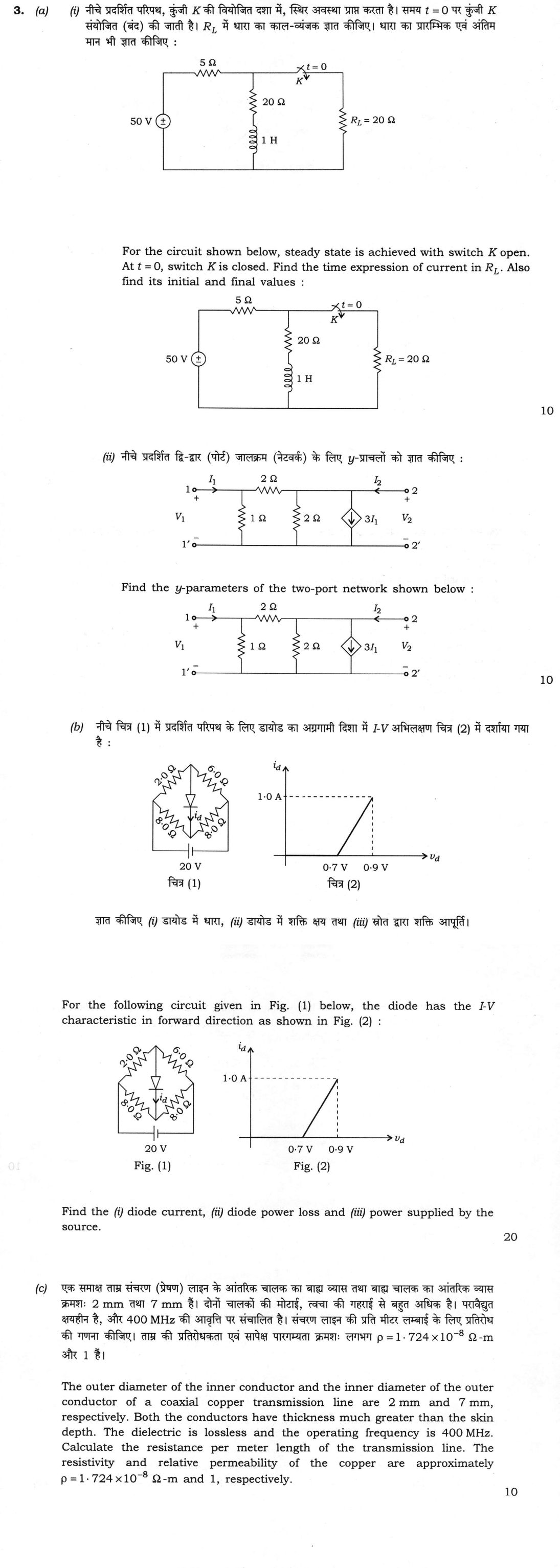
(a) (i) For the circuit shown below, steady state is achieved with switch K open. At t = 0, switch K is closed. Find the time…
For the circuit shown below, steady state is achieved with switch K open. At t = 0, switch K is closed. Find the time expression of current in R_L. Also find its initial and final values : 10 marks
Find the y-parameters of the two-port network shown below : 10 marks
For the following circuit given in Fig. (1) below, the diode has the I-V characteristic in forward direction as shown in Fig. (2) :
Fig. (1) Fig. 2 marks
Find the (i) diode current, (ii) diode power loss and (iii) power supplied by the source. 20 marks
The outer diameter of the inner conductor and the inner diameter of the outer conductor of a coaxial copper transmission line are 2 mm and 7 mm, respectively. Both the conductors have thickness much greater than the skin depth. The dielectric is lossless and the operating frequency is 400 MHz. Calculate the resistance per meter length of the transmission line. The resistivity and relative permeability of the copper are approximately ρ = 1·724 × 10⁻⁸ Ω-m and 1, respectively. 10 marks
हिंदी में प्रश्न पढ़ें
नीचे प्रदर्शित परिपथ, कुंजी K की वियोजित दशा में, स्थिर अवस्था प्राप्त करता है। समय t = 0 पर कुंजी K संयोजित (बंद) की जाती है। R_L में धारा का काल-व्यंजक ज्ञात कीजिए। धारा का प्रारम्भिक एवं अंतिम मान भी ज्ञात कीजिए : (10 अंक)
नीचे प्रदर्शित द्वि-द्वार (पोर्ट) जालक्रम (नेटवर्क) के लिए y-प्राचलों को ज्ञात कीजिए : (10 अंक)
नीचे चित्र (1) में प्रदर्शित परिपथ के लिए डायोड का अग्रगामी दिशा में I-V अभिलक्षण चित्र (2) में दर्शाया गया है :
चित्र (1) चित्र 2 अंक
ज्ञात कीजिए (i) डायोड में धारा, (ii) डायोड में शक्ति क्षय तथा (iii) स्रोत द्वारा शक्ति आपूर्ति। (20 अंक)
एक समाक्ष ताम्र संचरण (प्रेषण) लाइन के आंतरिक चालक का बाह्य व्यास तथा बाह्य चालक का आंतरिक व्यास क्रमशः 2 mm तथा 7 mm हैं। दोनों चालकों की मोटाई, त्वचा की गहराई से बहुत अधिक है। परावैद्युत क्षयहीन है, और 400 MHz की आवृत्ति पर संचालित है। संचरण लाइन की प्रति मीटर लम्बाई के लिए प्रतिरोध की गणना कीजिए। ताम्र की प्रतिरोधकता एवं सापेक्ष पारगम्यता क्रमशः लगभग ρ = 1·724 × 10⁻⁸ Ω-m और 1 हैं। (10 अंक)
Model answer
Drafted with AI by UPSC Answer Check against this question's marking rubric, to the expected length. UPSC does not publish answers for Mains — this is one way to score well, not an official key. How we build rubrics and answers.
(a)(i) Switching transient in the R_L circuit (10 marks)
Before t = 0 (K open). R_L is disconnected. The inductor acts as a short in steady state, so the 50 V source drives the 5 Ω resistor and the 20 Ω resistor in series: i_L(0⁻) = 50/(5 + 20) = 2 A.
After t = 0 (K closed). The inductor current cannot change instantly, so i_L(0⁺) = 2 A. The 5 Ω resistor, the 20 Ω load R_L and the source now form a network that feeds the 20 Ω + 1 H branch. Its Thevenin equivalent is
V_th = 50 × 20/(5 + 20) = 40 V and R_th = 5 ∥ 20 = 4 Ω.
For the inductor branch, R = R_th + 20 = 24 Ω, so the time constant is τ = L/R = 1/24 s, and the final inductor current is i_L(∞) = 40/24 = 5/3 A. Thus
i_L(t) = 5/3 + (2 − 5/3) e^(−24t) = 5/3 + (1/3) e^(−24t) A.
Current in R_L. The voltage across the branch (and hence across R_L) is v = 20 i_L + L di_L/dt. With di_L/dt = −8 e^(−24t) this gives
v(t) = 20 (5/3 + (1/3) e^(−24t)) − 8 e^(−24t) = 100/3 − (4/3) e^(−24t) V.
Therefore
i_RL(t) = v/20 = 5/3 − (1/15) e^(−24t) A ≈ 1.667 − 0.0667 e^(−24t) A, for t ≥ 0.
Initial and final values. i_RL(0⁺) = 5/3 − 1/15 = 1.6 A (check by KCL at 0⁺: (50 − v)/5 = v/20 + 2 gives v = 32 V and 32/20 = 1.6 A). Just before closing, i_RL = 0, so the current jumps to 1.6 A. i_RL(∞) = 5/3 ≈ 1.667 A (check: the total current 50/(5 + 10) = 10/3 A splits equally between the two 20 Ω paths).
(a)(ii) y-parameters of the two-port (10 marks)
Define I₁ = y₁₁V₁ + y₁₂V₂ and I₂ = y₂₁V₁ + y₂₂V₂. Node A (port 1) has a 1 Ω resistor to ground and a 2 Ω series resistor to node B (port 2). Node B has a 2 Ω resistor to ground and the dependent current source 3I₁ drawing current downward.
Port 1. I₁ = V₁/1 + (V₁ − V₂)/2 = 1.5V₁ − 0.5V₂.
Port 2. KCL at B: I₂ + (V₁ − V₂)/2 = V₂/2 + 3I₁, so
I₂ = V₂/2 + 3(1.5V₁ − 0.5V₂) − (V₁ − V₂)/2 = 4V₁ − 0.5V₂.
Hence
- y₁₁ = 1.5 S, y₁₂ = −0.5 S,
- y₂₁ = 4 S, y₂₂ = −0.5 S.
Check by short-circuit tests: with V₂ = 0, y₁₁ = 1 + 1/2 = 1.5 S; with V₂ = 0 the current 0.5V₁ enters node B from the series resistor and 3I₁ = 4.5V₁ leaves through the source, so I₂ = 4V₁ and y₂₁ = 4 S. The network is non-reciprocal (y₁₂ ≠ y₂₁) because of the dependent source, and y₂₂ is negative because the source sinks 3I₁ = 4.5V₁ − 1.5V₂.
(b) Diode in a resistive bridge (20 marks)
Circuit and diode model. The source is across the left and right corners, positive on the left, and the diode joins the top node T (junction of 2 Ω and 6 Ω) to the bottom node B (junction of the two 8 Ω resistors), conducting from T to B. Taking the source polarity as the one that forward-biases the diode (the reverse polarity would give a diode current of zero), the diode is an ideal 0.7 V drop plus a slope resistance: from Fig. (2), it starts conducting at 0.7 V and reaches 1.0 A at 0.9 V, so r_d = 0.2/1.0 = 0.2 Ω and v_d = 0.7 + 0.2 i_d for 0 ≤ i_d ≤ 1 A.
Thevenin equivalent seen by the diode. With the diode removed and the left corner at 20 V and the right at 0 V:
- V_T = 20 − 20 × 2/(2 + 6) = 15 V and V_B = 20 × 8/(8 + 8) = 10 V, so V_th = 15 − 10 = 5 V (T positive, so the diode is forward-biased);
- R_th = (2 ∥ 6) + (8 ∥ 8) = 1.5 + 4 = 5.5 Ω.
(i) Diode current. i_d = (V_th − 0.7)/(R_th + r_d) = (5 − 0.7)/(5.5 + 0.2) = 4.3/5.7 = 0.754 A, which lies within the linear range (below 1 A), and v_d = 0.7 + 0.2 × 0.754 = 0.851 V (below 0.9 V), confirming the region assumed.
(ii) Power loss in the diode. P_d = v_d i_d = 0.851 × 0.754 = 0.642 W.
(iii) Power supplied by the source. With V_B = 10 + 4 i_d = 13.02 V and V_T = V_B + v_d = 13.87 V, the source current is the sum of the currents in the two left-hand resistors: I_s = (20 − 13.87)/2 + (20 − 13.02)/8 = 3.066 + 0.873 = 3.939 A. The power supplied is P_s = 20 × 3.939 = 78.8 W.
Check. The resistors dissipate 3.066² × 2 = 18.80 W, 2.311² × 6 = 32.05 W, 0.873² × 8 = 6.09 W and 1.627² × 8 = 21.18 W. With the diode's 0.64 W the total is 78.8 W, equal to the source power.
(c) Resistance per metre of a coaxial copper line (10 marks)
At 400 MHz with conductors much thicker than the skin depth, the current flows in a thin surface layer and the resistance per unit length comes from the surface resistance. For copper with μ = μ₀ and ρ = 1.724 × 10⁻⁸ Ω·m:
R_s = √(πfμ₀ρ) = √(π × 400 × 10⁶ × 4π × 10⁻⁷ × 1.724 × 10⁻⁸) = 5.22 × 10⁻³ Ω per square.
The skin depth is δ = ρ/R_s = 3.30 μm, far below the conductor thicknesses, which justifies the surface-resistance approach.
The inner conductor has radius a = 1 mm and the outer conductor has inner radius b = 3.5 mm. The resistance per metre is the sum of the two conductors' contributions, each R_s divided by the circumference:
R = (R_s/2π)(1/a + 1/b) = (5.22 × 10⁻³/2π)(1/0.001 + 1/0.0035) = 8.30 × 10⁻⁴ × (1000 + 285.7) = 1.07 Ω/m.
The inner conductor contributes about 0.83 Ω/m and the outer about 0.24 Ω/m, since current density is highest on the smaller inner conductor.
How this answer will be evaluated
Evaluation rubric
Each sub-part is marked on its own, against the marks and word limit printed on the paper.
- (a)(i) Find the time expression of the current in R_L after K closes at t = 0 (steady state with K open), and its initial and final values. 10 marks
Must cover
- Inductor current before switching: 50/(5 + 20) = 2 A, continuous at t = 0
- Thevenin behind the inductor branch: 40 V and 4 Ω; τ = 1/24 s; i_L(∞) = 5/3 A
- i_RL(t) = 5/3 − (1/15)e^(−24t) A, from v = 20 i_L + L di_L/dt
- Initial value 1.6 A at 0⁺ (jump from 0) and final value 1.667 A
Loses marks
- Taking i_RL(0⁺) = 0 or 2 A.
- Using τ = L/20 or L/4 instead of L/24.
- Giving the inductor current instead of the R_L current.
Earns more
- KCL check at 0⁺ giving v = 32 V.
- Final-value check by current division.
Extra mark
- Sketch of i_RL(t) showing the jump from 0 to 1.6 A
- (a)(ii) Find y₁₁, y₁₂, y₂₁ and y₂₂ of the two-port containing a dependent current source 3I₁. 10 marks
Must cover
- Definition I₁ = y₁₁V₁ + y₁₂V₂, I₂ = y₂₁V₁ + y₂₂V₂
- Port 1: I₁ = 1.5V₁ − 0.5V₂, so y₁₁ = 1.5 S and y₁₂ = −0.5 S
- KCL at port-2 node with the source 3I₁ drawing current out of the node
- y₂₁ = 4 S and y₂₂ = −0.5 S
Loses marks
- Ignoring the dependent source in I₂.
- Sign error in the direction of the 3I₁ source.
- Assuming reciprocity, y₁₂ = y₂₁.
Earns more
- Short-circuit check of y₁₁ and y₂₁.
- Comment that y₁₂ ≠ y₂₁ (non-reciprocal because of the dependent source).
Extra mark
- Conversion of the y-matrix to another parameter set for verification
- (b) For the diode-bridge circuit with the given piecewise-linear diode characteristic, find the diode current, the diode power loss and the power supplied by the source. 20 marks
Must cover
- Diode model from Fig. (2): v_d = 0.7 + 0.2 i_d for 0 ≤ i_d ≤ 1 A, r_d = 0.2 Ω
- Thevenin across the diode: V_th = 5 V, R_th = (2∥6) + (8∥8) = 5.5 Ω
- i_d = 4.3/5.7 = 0.754 A with v_d = 0.851 V, both in range
- Diode power 0.642 W; source power ≈ 78.8 W from I_s = 3.94 A
Loses marks
- Treating the diode as an ideal switch with no drop or resistance.
- Using the resistors in the wrong series-parallel arrangement for R_th.
- Computing source power without including the current through the 8 Ω resistor.
Earns more
- Statement of the source polarity that makes the diode conduct.
- Power-balance check over all resistors and the diode.
Extra mark
- Check that the diode remains in the linear region
- (c) Calculate the resistance per metre of a coaxial copper line at 400 MHz with inner conductor diameter 2 mm and outer conductor inner diameter 7 mm. 10 marks
Must cover
- Skin effect: R_s = √(πfμ₀ρ) = 5.22 × 10⁻³ Ω per square
- Skin depth 3.3 μm much less than the thickness, so surface resistance applies
- Radii a = 1 mm and b = 3.5 mm
- R = (R_s/2π)(1/a + 1/b) ≈ 1.07 Ω/m
Loses marks
- Using diameters instead of radii.
- Using DC resistance instead of the skin-effect resistance.
- Using μ = 1 instead of μ₀ = 4π × 10⁻⁷ in R_s.
Earns more
- Separate contributions of the inner (0.83 Ω/m) and outer (0.24 Ω/m) conductors.
Extra mark
- Statement of the general formula for the coaxial line's series resistance
What "State" is asking you to do
Give the formulation itself — the theorem, rule, statutory provision or position — worded accurately. Precision of wording is the whole of the mark; no background or justification is being asked for.
Structure that answers it
The statement in full, complete in itself → the conditions under which it holds → an illustration only where the stem asks for one
Where marks are lost
Approximating the wording. A theorem or a provision stated loosely forfeits the mark that exact statement would have carried.
Practice this exact question
Write your answer and it is marked point by point against the model answer above — what you covered, what you missed, what you got wrong.
Evaluate my answer →More from Electrical Engineering 2026 Paper I
- Q1 (a) For the circuit shown below, if the power loss in 1 Ω resistor is 16 W, find the valu…
- Q2 (a) (i) Find the values of R and C in the figure shown below, so that V_b = 3V_a, also V̄…
- Q3 (a) (i) For the circuit shown below, steady state is achieved with switch K open. At t =…
- Q4 (a) (i) The continuous-time signal x(t) = cos(20πt + π/4) is ideally sampled at a rate of…
- Q5 (a) For the circuit given in the figure below, the input voltage signal is given by V_in…
- Q6 (a) Design a MOD-6 synchronous DOWN counter using J-K flip-flops. (20 marks) (b) A three-…