Paper II — Q2
(a) Determine the response of the system shown in the following figure when it is excited by a unit step input. (20 marks) (b)…
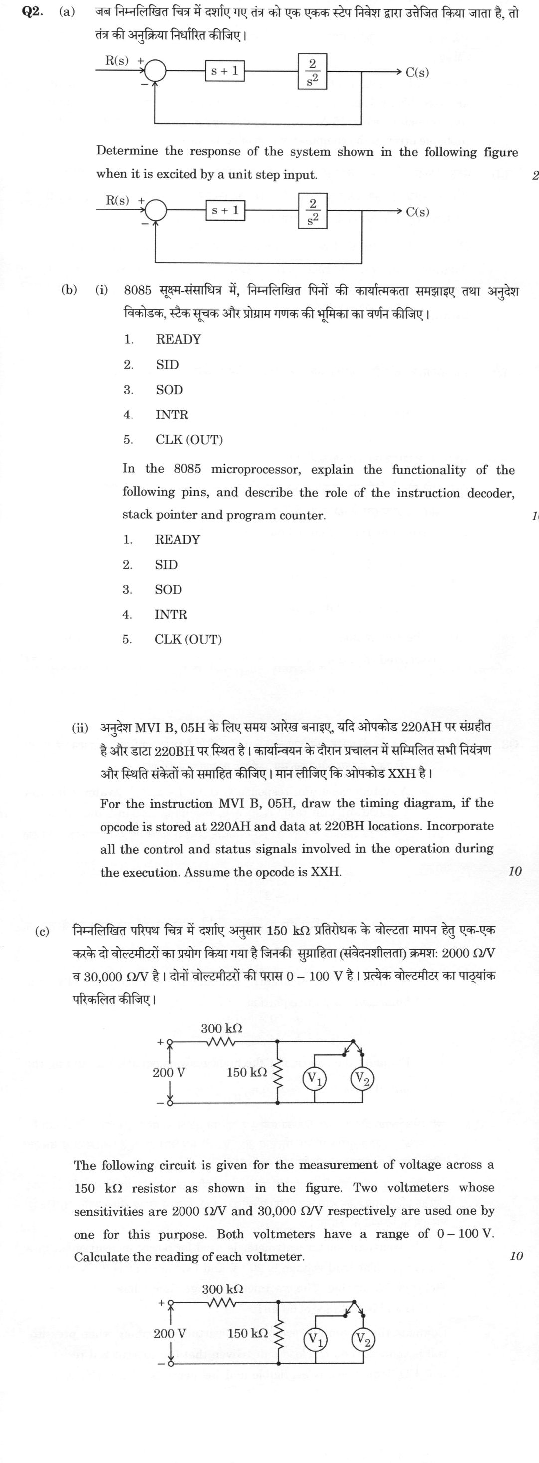
Determine the response of the system shown in the following figure when it is excited by a unit step input. 20 marks
In the 8085 microprocessor, explain the functionality of the following pins, and describe the role of the instruction decoder, stack pointer and program counter. 1. READY 2. SID 3. SOD 4. INTR 5. CLK (OUT) 10 marks
For the instruction MVI B, 05H, draw the timing diagram, if the opcode is stored at 220AH and data at 220BH locations. Incorporate all the control and status signals involved in the operation during the execution. Assume the opcode is XXH. 10 marks
The following circuit is given for the measurement of voltage across a 150 kΩ resistor as shown in the figure. Two voltmeters whose sensitivities are 2000 Ω/V and 30,000 Ω/V respectively are used one by one for this purpose. Both voltmeters have a range of 0 – 100 V. Calculate the reading of each voltmeter. [Figure: circuit diagram with 300 kΩ, 200 V, 150 kΩ, V₁, V₂] 10 marks
हिंदी में प्रश्न पढ़ें
जब निम्नलिखित चित्र में दर्शाए गए तंत्र को एक एकल स्टेप निवेश द्वारा उत्तेजित किया जाता है, तो तंत्र की अनुक्रिया निर्धारित कीजिए। (20 अंक)
8085 सूक्ष्म-संसाधित्र में, निम्नलिखित पिनों की कार्यात्मकता समझाइए तथा अनुदेश विकोडक, स्टैक सूचक और प्रोग्राम गणक की भूमिका का वर्णन कीजिए। 1. READY 2. SID 3. SOD 4. INTR 5. CLK (OUT) (10 अंक)
अनुदेश MVI B, 05H के लिए समय आरेख बनाइए, यदि ऑपकोड 220AH पर संग्रहीत है और डाटा 220BH पर स्थित है। कार्यान्वयन के दौरान प्रचालन में सम्मिलित सभी नियंत्रण और स्थिति संकेतों को समाहित कीजिए। मान लीजिए कि ऑपकोड XXH है। (10 अंक)
निम्नलिखित परिपथ चित्र में दर्शाए अनुसार 150 kΩ प्रतिरोधक के वोल्टता मापन हेतु एक-एक करके दो वोल्टमीटरों का प्रयोग किया गया है जिनकी सुग्राहिता (संवेदनशीलता) क्रमश: 2000 Ω/V व 30,000 Ω/V है। दोनों वोल्टमीटरों की परास 0 – 100 V है। प्रत्येक वोल्टमीटर का पाठ्यांक परिकलित कीजिए। [चित्र: 300 kΩ, 200 V, 150 kΩ, V₁, V₂ वाले परिपथ आरेख] (10 अंक)
Model answer
Drafted with AI by UPSC Answer Check against this question's marking rubric, to the expected length. UPSC does not publish answers for Mains — this is one way to score well, not an official key. How we build rubrics and answers.
(a) Step response of the unity-feedback system (20 marks)
The forward path is G(s) = (s + 1) × 2/s² = 2(s + 1)/s², with unity negative feedback (H = 1). The closed-loop transfer function is
C(s)/R(s) = G/(1 + G) = 2(s + 1)/(s² + 2s + 2).
Comparing the denominator with s² + 2ζω_n s + ω_n²: ω_n = √2 = 1.414 rad/s and ζ = 1/√2 = 0.707, so the system is under-damped, with a zero at s = −1 and poles at s = −1 ± j1.
For a unit step, R(s) = 1/s, so
C(s) = 2(s + 1)/[s(s² + 2s + 2)] = A/s + (Bs + D)/(s² + 2s + 2).
Then A = 2(1)/2 = 1, and equating coefficients of 2(s + 1) = (s² + 2s + 2) + (Bs + D)s gives B = −1 and D = 0. Hence
C(s) = 1/s − s/[(s + 1)² + 1] = 1/s − (s + 1)/[(s + 1)² + 1] + 1/[(s + 1)² + 1].
Taking the inverse Laplace transform:
c(t) = 1 − e^(−t) cos t + e^(−t) sin t = 1 + e^(−t)(sin t − cos t), for t ≥ 0.
Checks. c(0) = 1 + (0 − 1) = 0, and the final value is c(∞) = 1, so the steady-state error to a unit step is zero. The derivative is c′(t) = 2e^(−t) cos t, which is zero at t = π/2 = 1.571 s. Hence the peak time is t_p = 1.571 s and the peak value is c(t_p) = 1 + e^(−π/2) = 1.208, a peak overshoot of 20.8%. The settling time (2% band) is about 4/(ζω_n) = 4/1 = 4 s, and the response is oscillatory, decaying with the envelope e^(−t).

(b)(i) 8085 pins and the internal registers (10 marks)
- READY (input). A slow memory or peripheral pulls READY low to say that it is not ready to send or accept data. The microprocessor samples it in T₂ of a read or write cycle and, if it is low, inserts wait states until it goes high, which lets fast processors work with slow devices.
- SID (serial input data, input). A serial data line. The bit present on SID is loaded into bit 7 of the accumulator when the RIM instruction is executed.
- SOD (serial output data, output). A serial data line. When the SIM instruction is executed with the serial-output enable bit (D₆) set, bit 7 of the accumulator is latched to SOD.
- INTR (interrupt request, input). A general-purpose, maskable, non-vectored, level-sensitive interrupt. It is sampled in the last T-state of each instruction, and it is recognised only if interrupts are enabled (EI). The processor then issues INTA and the device supplies an instruction, normally RST n or CALL, to which the processor branches.
- CLK (OUT), output. The system clock output, at half the frequency of the crystal or LC circuit on X₁ and X₂ (3 MHz for a 6 MHz crystal). It drives clock inputs of peripherals and synchronises the system.
Instruction decoder. The opcode fetched in the opcode-fetch cycle is held in the instruction register and decoded by the instruction decoder. The decoder, with the timing and control unit, decides the machine cycles and the control signals (RD, WR, ALE, IO/M, S₀, S₁) needed to execute the instruction.
Stack pointer (SP). A 16-bit register that points to the top of the stack, a last-in first-out area of read/write memory. It is decremented by 2 on PUSH or CALL, when data or the return address are saved, and incremented by 2 on POP or RET. It is also used to save the program counter when an interrupt is accepted.
Program counter (PC). A 16-bit register that holds the address of the next instruction to be fetched. It is incremented automatically after each byte is fetched, so the program is executed sequentially, and it is loaded with a new address by jump, call, return and interrupt operations. The 8085 can address 64 KB of memory through the PC.
(b)(ii) Timing diagram for MVI B, 05H (10 marks)
MVI B, 05H is a two-byte instruction: the opcode (06H, written XXH as instructed) at 220AH and the data 05H at 220BH. It needs two machine cycles and seven T-states:
- M₁, opcode fetch (T₁ to T₄). In T₁ the processor places 22H on A₁₅–A₈ and 0AH on AD₇–AD₀, and ALE goes high in T₁ so that an external latch can hold the low-order address. IO/M = 0 (memory access; RD and WR are active low), and the status signals are S₁S₀ = 11 (opcode fetch). RD goes low from T₂ to T₃ and the memory places the opcode on AD₇–AD₀, which the processor latches at the end of T₃. In T₄ the opcode is decoded; RD is high and WR remains high.
- M₂, memory read (T₁ to T₃). The PC now holds 220BH. In T₁ the address 22H, 0BH appears on the buses with ALE high, IO/M = 0 and S₁S₀ = 10 (memory read). RD is low in T₂ and T₃, and the data byte 05H is placed on AD₇–AD₀ and read into register B at the end of T₃.
READY is held high (no wait state) and WR stays high (inactive) throughout, since there is no write.

(c) Loading error of voltmeters (10 marks)
Input resistances. Each voltmeter's resistance is its sensitivity times its range: V₁ = 2000 Ω/V × 100 V = 200 kΩ, and V₂ = 30 000 Ω/V × 100 V = 3 MΩ.
True voltage without a meter. The 150 kΩ resistor with the 300 kΩ series resistor across the 200 V source has V = 200 × 150/(300 + 150) = 66.67 V.
Reading of V₁. The meter is in parallel with the 150 kΩ resistor: R_p = 150 × 200/(150 + 200) = 85.71 kΩ. Then
V₁ = 200 × 85.71/(300 + 85.71) = 44.4 V.
Reading of V₂. R_p = 150 × 3000/(150 + 3000) = 142.86 kΩ, so
V₂ = 200 × 142.86/(300 + 142.86) = 64.5 V.
The loading error is (44.4 − 66.7)/66.7 = −33.3% for V₁ and (64.5 − 66.7)/66.7 = −3.2% for V₂, which shows that a high-sensitivity meter is needed for a high-resistance circuit.
How this answer will be evaluated
Evaluation rubric
Each sub-part is marked on its own, against the marks and word limit printed on the paper.
- (a) Determine the unit-step response of the unity-feedback system with (s + 1) and 2/s² in the forward path. 20 marks
Must cover
- Closed-loop transfer function C/R = 2(s + 1)/(s² + 2s + 2)
- C(s) = 2(s + 1)/[s(s² + 2s + 2)] and partial fractions 1/s − s/((s + 1)² + 1)
- c(t) = 1 + e^(−t)(sin t − cos t) for t ≥ 0
- Checks: c(0) = 0, c(∞) = 1, ζ = 0.707, peak 1.208 at 1.571 s
Loses marks
- Using G(s) instead of the closed-loop function.
- Arithmetic errors in the partial fractions (wrong sign of the e^(−t) terms).
- Omitting the zero at s = −1 from the numerator.
Earns more
- ω_n = √2 and ζ = 0.707 identified.
- Sketch of the response with the overshoot marked.
Extra mark
- Peak overshoot 20.8% and settling time about 4 s
- (b)(i) Explain the functions of the READY, SID, SOD, INTR and CLK (OUT) pins of the 8085 and describe the roles of the instruction decoder, stack pointer and program counter. 10 marks
Must cover
- READY: input for slow devices, wait states; SID and SOD: serial input and output via RIM and SIM
- INTR: maskable, level-sensitive, non-vectored interrupt request sampled at the end of each instruction, enabled by EI
- CLK (OUT): system clock at half the crystal frequency
- Instruction decoder (decodes the opcode and drives control signals), 16-bit SP (top of stack, PUSH/POP/CALL/RET), 16-bit PC (next instruction address)
Loses marks
- Describing INTR as non-maskable or vectored.
- Confusing SID with SOD or the clock with the crystal frequency.
- Describing the stack pointer as holding the next instruction.
Earns more
- Naming the instructions RIM and SIM for SID and SOD.
- INTA and RST n response after INTR.
Extra mark
- Mention of the 3 MHz clock for a 6 MHz crystal
- (b)(ii) Draw the 8085 timing diagram for MVI B, 05H with the opcode at 220AH and data at 220BH, showing all control and status signals. 10 marks
Must cover
- Two machine cycles: opcode fetch M₁ (4 T-states) and memory read M₂ (3 T-states), 7 T-states in all
- Address 22H on A₁₅–A₈ and low byte 0AH (then 0BH) on AD₇–AD₀ with ALE high in T₁
- IO/M = 0; S₁S₀ = 11 in M₁ and 10 in M₂; RD low in T₂–T₃ of each cycle; WR stays high
- Opcode XXH read in M₁ and decoded in T₄; data 05H read in M₂
Loses marks
- Showing WR asserted or an I/O cycle (IO/M high).
- Omitting the T₄ state of the opcode fetch.
- Using three machine cycles.
Earns more
- READY shown high (no wait states).
- Correct labelling of the clock and T-states.
Extra mark
- Statement of the actual opcode 06H
- (c) Calculate the reading of each of two voltmeters (2000 Ω/V and 30 000 Ω/V, range 0–100 V) used to measure the voltage across the 150 kΩ resistor in the 200 V, 300 kΩ circuit. 10 marks
Must cover
- Input resistances 200 kΩ and 3 MΩ
- Voltmeter in parallel with 150 kΩ (85.7 kΩ and 142.9 kΩ)
- V₁ = 44.4 V and V₂ = 64.5 V
- True voltage 66.7 V, so loading errors of about −33% and −3%
Loses marks
- Ignoring the meter resistance and giving 66.7 V for both.
- Using the range 100 V as the resistance.
- Placing the meter in series with the resistor.
Earns more
- Comparison with the unloaded value and percentage errors.
Extra mark
- Conclusion on the need for a high-sensitivity voltmeter
What "Calculate" is asking you to do
Apply the standard formula or schedule to data the question has already supplied — a table of readings, cost records, a balance sheet — and produce the number. The method is rarely in doubt; the marks sit in the named intermediate quantities, each of which has to appear as a labelled line.
Structure that answers it
Data as given → formula or standard treatment, named → substitution → each intermediate, labelled → result with units
Where marks are lost
Omitting an intermediate the marking scheme pays for separately, or rounding at an intermediate line so the final figure drifts. In commerce and accountancy, any figure in a statement that no numbered working note supports is treated as unearned.
Practice this exact question
Write your answer and it is marked point by point against the model answer above — what you covered, what you missed, what you got wrong.
Evaluate my answer →More from Electrical Engineering 2026 Paper II
- Q1 (a) A unity feedback system has open loop transfer function G(s) = \frac{K}{s(s+q)}. Eval…
- Q2 (a) Determine the response of the system shown in the following figure when it is excited…
- Q3 (a) (i) A system has a unit response as c(t) = 1 − e^(−0·5t). Evaluate its unit impulse a…
- Q4 (a) Design a PI controller so that a unity feedback system having open loop transfer func…
- Q5 (a) Write the state space equation for the following circuit. [Circuit diagram: voltage s…