GS Paper III — Q16
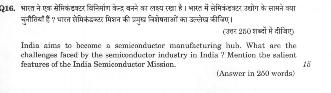
India aims to become a semiconductor manufacturing hub. What are the challenges faced by the semiconductor industry in India ?…
India aims to become a semiconductor manufacturing hub. What are the challenges faced by the semiconductor industry in India ? Mention the salient features of the India Semiconductor Mission. (Answer in 250 words) 15 marks
हिंदी में प्रश्न पढ़ें
भारत ने एक सेमीकंडक्टर विनिर्माण केन्द्र बनने का लक्ष्य रखा है। भारत में सेमीकंडक्टर उद्योग के सामने क्या चुनौतियाँ हैं ? भारत सेमीकंडक्टर मिशन की प्रमुख विशेषताओं का उल्लेख कीजिए। (उत्तर 250 शब्दों में दीजिए)
Model answer
Written by UPSC Answer Check against this question's marking rubric, to the 250-word length. UPSC does not publish answers for Mains — this is one way to score well, not an official key.
India’s push to become a semiconductor hub is strategic for digital sovereignty, defence and green-tech supply chains, but the industry faces structural constraints. Challenges: Fab construction is highly capital intensive, with advanced facilities costing $5–10 billion, and long gestation periods deter private investment. India lacks a complete ecosystem: fab-grade silicon wafer manufacturing, specialty chemicals, gases and raw materials are largely imported. Skilled talent in chip design, process engineering and fabrication is scarce, while power and water reliability remain uneven. Geopolitical technology denial regimes restrict access to advanced lithography and IP, and fragmented global supply chains expose India to bottlenecks. R&D spending is also limited compared with global leaders.
India Semiconductor Mission: Launched under the Semicon India Programme, the $10 billion mission offers fiscal support up to 50% of project cost for silicon and display fabs, and up to 30% for ATMP/OSAT, compound semiconductors, silicon photonics, sensors and discrete semiconductors; design-linked incentives for design companies are separate. It establishes the India Semiconductor Research Centre, prioritises mature-node (28nm+) manufacturing initially, and promotes state partnerships in Gujarat, Tamil Nadu and Assam. The mission integrates design, fabrication, packaging and testing. Recent approvals and state-level proposals include Micron’s ATMP unit (Assembly, Testing, Marking and Packaging) in Gujarat, Tata-CG Power (CG Power-Renesas) in Gujarat, Tata-PSMC in Gujarat, Tata OSAT in Assam, and ISMC Digital in Karnataka.
With sustained power, water, skills and IP support, India can convert mission incentives into a resilient semiconductor value chain.
What "Mention" is asking you to do
Put specific factual content on record — the names, features, targets or instances the stem asks for. Mention is usually the subordinate half of a larger question, so it must be done fully but quickly, leaving room for the part that carries the main directive.
Structure that answers it
The items named directly, without preamble → one qualifying detail against each → straight on to the part of the stem the marks actually sit in
Where marks are lost
Gesturing at the category instead of naming the particulars, or expanding it until the analytical half of the question is squeezed.
How this answer will be evaluated
Approach
Framework: Situation > Analysis > Measures > Assessment. challenges: 3-4 challenges > solutions mapped to them > conclusion | highlight: name the salient points > one line of substance each > close Full marks: Precise technical challenges mapped to ISM features with specific data.
Key points expected
- High capital intensity of fabrication plants
- Lack of specialized skilled workforce
- Dependence on imported raw materials/equipment
- Complex regulatory and land acquisition hurdles
- Financial support for manufacturing units
- Incentives for R&D and design centers
- Establishment of India Semiconductor Council
- Support for ancillary and packaging industries
Evaluation rubric
Each sub-part is marked on its own, against the marks and word limit printed on the paper.
- The answer Identify 3-4 specific industry challenges and map them to solutions. · 250 words
challenges— 3-4 challenges → solutions mapped to them → conclusion
Must cover
- High capital intensity of fabrication plants
- Lack of specialized skilled workforce
- Dependence on imported raw materials/equipment
- Complex regulatory and land acquisition hurdles
Loses marks
- Generic economic challenges not specific to semis
- Listing challenges without any solution mapping
Earns more
- Mention of water and power infrastructure gaps
- Reference to global supply chain volatility
- Lack of domestic R&D ecosystem
Extra mark
- Citing specific cost figures for a fab
- Mentioning specific water-intensive processes
- The answer List salient features of the India Semiconductor Mission (ISM). · 250 words
highlight— name the salient points → one line of substance each → close
Must cover
- Financial support for manufacturing units
- Incentives for R&D and design centers
- Establishment of India Semiconductor Council
- Support for ancillary and packaging industries
Loses marks
- Confusing ISM with general IT policies
- Vague description of 'government support'
Earns more
- Mention of specific budget allocation (e.g., ₹76,000 Cr)
- Reference to 'Make in India' linkage
- Mention of talent development initiatives
Extra mark
- Citing the specific year of launch (2021)
- Mentioning the specific percentage of capex support
Practice this exact question
Write your answer and it is marked point by point against the model answer above — what you covered, what you missed, what you got wrong.
Evaluate my answer →More from General Studies 2025 GS Paper III
- Q13 Examine the factors responsible for depleting groundwater in India. What are the steps ta…
- Q14 Examine the scope of the food processing industries in India. Elaborate the measures take…
- Q15 How does nanotechnology offer significant advancements in the field of agriculture ? How…
- Q16 India aims to become a semiconductor manufacturing hub. What are the challenges faced by…
- Q17 Mineral resources are fundamental to the country's economy and these are exploited by min…
- Q18 Write a review on India's climate commitments under the Paris Agreement (2015) and mentio…
- Q19 What are the major challenges to internal security and peace process in the North-Eastern…